- P6 (microarchitecture)
-
The P6 microarchitecture is the sixth generation Intel x86 microarchitecture, implemented by the Pentium Pro microprocessor that was introduced in November 1995. It is sometimes referred to as i686.[citation needed] It was succeeded by the NetBurst microarchitecture in 2000, but eventually revived in the Pentium M line of microprocessors. The successor to the Pentium M variant of the P6 microarchitecture is the Core microarchitecture.
Contents
From Pentium Pro to Pentium III
The P6 core was the sixth generation Intel microprocessor in the x86 space. The first implementation of the P6 core was the Pentium Pro CPU in 1995, the immediate successor to the original Pentium design (P5).
Some techniques first used in the x86 space in the P6 core include:
- Speculative execution and out-of-order completion (called "dynamic execution" by Intel), which required new retire units in the execution core. This lessened pipeline stalls, and in part enabled greater speed-scaling of the Pentium Pro and successive generations of CPUs.
- Superpipelining, which increased from Pentium's 5-stage pipeline to 14 of the Pentium Pro, and eventually morphed into the 10-stage pipeline of the Pentium III, and the 12- to 14-stage pipeline of the Pentium M.
- PAE and wider 36-bit address bus to support 64 GB of physical memory (the linear address space of a process was still limited to 4 GB).
- Register renaming, which enabled more efficient execution of multiple instructions in the pipeline.
- CMOV instructions heavily used in compiler optimization.
The P6 architecture lasted three generations from the Pentium Pro to Pentium III, and was widely known for low power consumption, excellent integer performance, and relatively high instructions per cycle (IPC). When the new NetBurst (P68) architecture was conceived, initially in the Willamette core, which had relatively low IPC and less efficient overall design both in terms of power consumption and throughput efficiency, the P6 line of processing cores were largely thought to be abandoned.
Revived microarchitecture in Pentium M (Banias and Dothan)
Upon release of the Pentium 4-M and Mobile Pentium 4, it was quickly realized that the new mobile NetBurst processors were not ideal for mobile computing. The Netburst-based processors were simply not as efficient per clock or per watt compared to their P6 predecessors. Mobile Pentium 4 processors ran much hotter than Pentium III-M processors and didn't offer significant performance advantages. Its inefficiency affected not only the cooling system complexity, but also the all-important battery life.
Realizing their new microarchitecture wasn't the best choice for the mobile space, Intel went back to the drawing board for a design that would be optimally suited for this market segment. The result was a hybrid, and at the time, modernized P6 design called the Pentium M:
Design Overview[1]
- Quad-pumped Front Side Bus. With the initial Banias core, Intel adopted the 400 MHz FSB first used in the Pentium 4. The Dothan core moved to the 533 MHz FSB, following the Pentium 4's evolution.
- Larger L2 cache. Initially 1 MB in the Banias core, then 2 MB in the Dothan core. Dynamic cache activation by quadrant selector from sleep states.
- SSE2 Streaming SIMD (Single Instruction, Multiple Data) Extensions 2 support.
- A 12-14-stage instruction pipeline to achieve higher clock speeds than the Pentium III-M.
- Dedicated register stack management.
- Addition of global history to branch prediction table.
- Micro-ops Fusion of certain sub-instructions mediated by decoding units. x86 commands can be combined into fewer RISC micro operations.
The Pentium M was the most power efficient x86 processor for notebooks for several years, consuming a maximum of 27 watts at maximum load and 4-5 watts while idle. The processing efficiency gains brought about by its modernization allowed it to rival the Mobile Pentium 4 clocked over 1 GHz higher (the fastest-clocked Mobile Pentium 4 compared to the fastest-clocked Pentium M) and equipped with much more memory and bus bandwidth.[1]
Intel Core (Yonah)
Main article: Yonah (microprocessor)The Yonah CPU was launched in January 2006 under the Core brand. Single and dual-core mobile version were sold under the Core Solo, Core Duo, and Pentium Dual-Core brands, and a server version was released as Xeon LV. These processors provided partial solutions to some of the foregoing Pentium M's shortcomings, by adding to its P6 microarchitecture:
- SSE3 Support
- Single- and dual-core technology with 2 MB of shared L2 cache (restructuring processor organization)
- Increased FSB speed, with the FSB running at 533 MHz or 667 MHz.
- A 12-stage instruction pipeline.
This resulted in the interim microarchitecture for low-voltage only CPUs, part way between P6 and the following Core microarchitecture.
Successor
Main article: Intel Core (microarchitecture)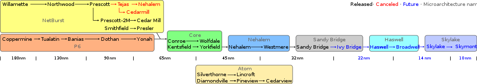 Intel CPU core roadmaps from NetBurst and P6 to Skylake
On July 27, 2006, the Core microarchitecture, a distant relative of P6, was launched in form of the Core 2 processor. Subsequently, more processors were released with the Core microarchitecture under Core 2, Xeon, Pentium and Celeron brand names. The Core microarchitecture is Intel's final mainstream processor line to use FSB, with all later Intel processors based on Nehalem and following Intel microarchitectures exclusively using the QPI or DMI bus. Improvements from the Intel Core processors were:
- A 14-stage instruction pipeline to achieve significantly higher clock speeds than the Core processsors.
- SSSE3 support for all models and SSE4.1 support for all Core 2 models manufactured at a 45 nm lithography.
- An x86-64 (64-bit) instruction set is added, allowing all Core 2 processors to run 64-bit applications.
- Increased FSB speed, with the FSB running from 533 MHz to 1600 MHz.
- Increased L2 cache size, with the L2 cache size ranging from 1 MB to 12 MB (Core 2 Duo processors use a shared L2 cache with Core 2 Quad processors having half of the total cache allocated to each die).
- Some mobile Core 2 Duo processors support Dynamic Front Side Bus Throttling, with the FSB running at half of its full speed in Super Low Frequency Mode, therefore reducing the core speed to half of its full speed as well. This technique allows the processors to consume less power, increasing battery life.
- Some mobile Core 2 Duo processors have Dynamic Acceleration Technology, while mobile Core 2 Quad processors support Dual Dynamic Acceleration Technology. For a mobile Core 2 Duo, this feature allows the CPU to overclock one processor core while turning off the other one. As for a mobile Core 2 Quad, two cores can be overclocked. The processor does this if an application only uses a single core or two as a minimum requirement to function effectively and the clock multiplier is only increased by 1.
P6 based chips
- Celeron (Covington/Mendocino/Coppermine/Tualatin variants)
- Pentium Pro
- Pentium II Overdrive (a Pentium II chip in the 387 pin Socket 8)
- Pentium II
- Pentium II Xeon
- Pentium III
- Pentium III Xeon
Banias/Dothan variant
Yonah variant
- Celeron M 400 series
- Core Solo/Duo
- Pentium Dual-Core T2060/T2080/T2130
- Xeon LV/ULV (Sossaman)
While all these chips are technically derivatives of the Pentium Pro the architecture has gone through several radical changes since its inception.[2]
See also
- Core microarchitecture
- Bob Colwell
- List of Intel CPU microarchitectures
References
- ^ a b Lal Shimpi, Anand. Intel's 90nm Pentium M 755: Dothan Investigated, AnandTech, July 21, 2004.
- ^ Pat Gelsinger talk at Stanford, Jun 7th 2006
Intel processors Discontinued BCD oriented (4-bit) pre-x86 (8-bit) Early x86 (16-bit) x87 (external FPUs) IA-32 (32-bit) x86-64 (64-bit) Other Current Lists Microarchitectures P5 P5 based cores 800 nm - P5
600 nm - P54C
350 nm - P54CS
- P55C
250 nm - Tillamook
P6 P6 / Pentium M / Enhanced Pentium M based cores 500 nm 350 nm - P6
- Klamath
250 nm - Mendocino
- Dixon
- Tonga
- Covington
- Deschutes
- Katmai
- Drake
- Tanner
180 nm - Coppermine
- Coppermine T
- Timna
- Cascades
130 nm - Tualatin
- Banias
90 nm - Dothan
- Stealey
65 nm - Tolapai
- Yonah
- Sossaman
NetBurst NetBurst based cores 180 nm 130 nm 90 nm 65 nm Core Core / Penryn based cores 65 nm 45 nm - Penryn
- Penryn-QC
- Wolfdale
- Yorkfield
- Wolfdale-DP
- Harpertown
- Dunnington
Bonnell Bonnell based cores 45 nm - Silverthorne
- Diamondville
- Pineview
- Lincroft
- Tunnel Creek
- Sodaville
32 nm - Cedarview
- Cedar Trail-M
Nehalem Nehalem / Westmere based cores 45 nm - Clarksfield
- Lynnfield
- Jasper Forest
- Bloomfield
- Gainestown (Nehalem-EP)
- Beckton (Nehalem-EX)
32 nm - Arrandale
- Clarkdale
- Gulftown (Westmere-EP)
- Westmere-EX
Sandy Bridge Sandy Bridge / Ivy Bridge based cores 32 nm - Sandy Bridge
Future Categories:- Intel x86 microprocessors

Wikimedia Foundation. 2010.