- Multijunction photovoltaic cell
-
Multi-junction solar cells or tandem cells are solar cells containing several p-n junctions. Each junction is tuned to a different wavelength of light, reducing one of the largest inherent sources of losses, and thereby increasing efficiency. Traditional single-junction cells have a maximum theoretical efficiency of 34%, a theoretical "infinite-junction" cell would improve this to 87% under highly concentrated sunlight.
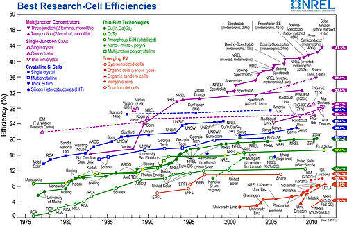
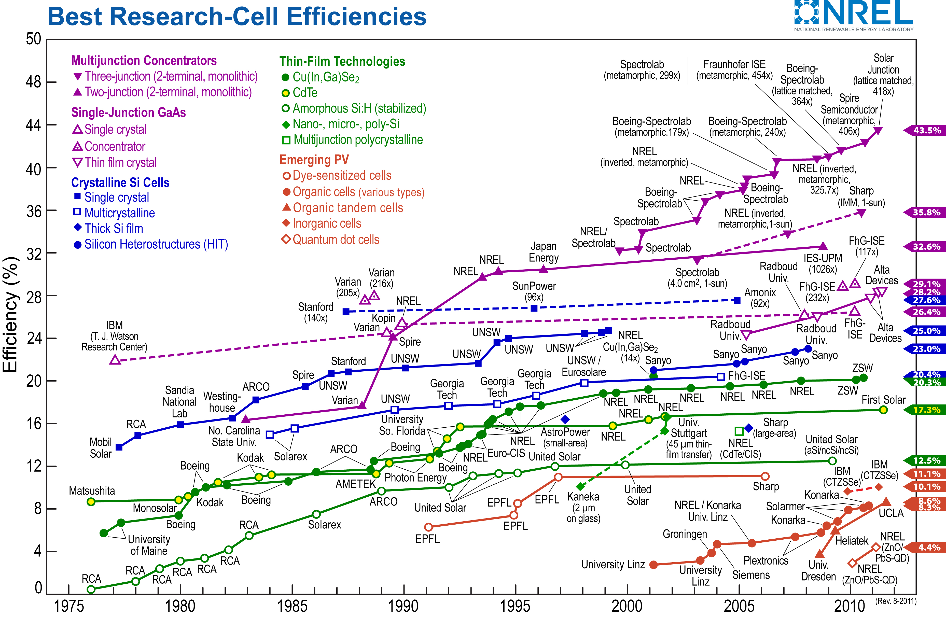
Currently, the best lab examples of traditional silicon solar cells have efficiencies around 25%[1], while lab examples of multi-junction cells have demonstrated performance over 42%.[2] Commercial examples of tandem cells are widely available at 30% under one-sun illumination,[3] and improve to around 40% under concentrated sunlight. However, this efficiency is gained at the cost of increased complexity and manufacturing price. To date, their higher price and lower price-to-performance ratio have limited their use to special roles, notably in aerospace where their high power-to-weight ratio is desirable. In terrestrial applications these solar cells are used in concentrated photovoltaics (CPV)[4] with operating plants all over the world [5].
Tandem techniques can also be used to improve the performance of existing cell designs, although there are strict limits in the choice of materials. In particular, the technique can be applied to thin-film solar cells using amorphous silicon to produce a cell with about 10% efficiency that is lightweight and flexible. This approach has been used by several commercial vendors,[6] but these products are currently limited to certain niche roles, like roofing materials.
Contents
Description
Basics of solar cells
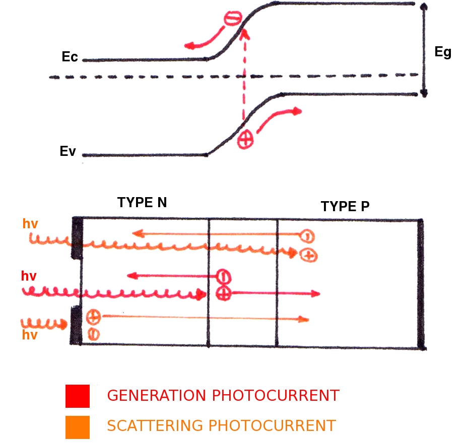
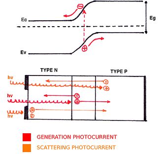 Figure A. Schematic illustration of the photovoltaic effect. Photons give their energy to electrons in the depletion or quasi-neutral regions. These move from conduction band to valence band. Depending of the location, electrons and holes are accelerated by Edrift, which gives generation photocurrent, or by Escatt, which gives scattering photocurrent.[7]
Traditional photovoltaic cells are commonly composed by doped silicon and then depositing metallic contacts on the top and bottom. The doping is normally applied to a thin layer on the top of the cell, producing a pn-junction with a particular bandgap energy, Eg.
Photons that hit the top of the solar cell are either reflected or transmitted. Transmitted photons have the potential to give their energy hν to an electron if hν ≥ Eg, generating an electron-hole pair.[8] In the depletion region, the drift electric field Edrift accelerates both electrons and holes towards their respective n-doped and p-doped regions (up and down, respectively). The resulting current Ig is called the generation photocurrent. In the quasi-neutral region, the scattering electric field Escatt accelerates holes (electrons) towards the p-doped (n-doped) region, which gives a scattering photocurrent Ipscatt (Inscatt). Consequently, due to the accumulation of charges, a potential V and a photocurrent Iph appear. The expression for this photocurrent is obtained by adding generation and scattering photocurrents: Iph = Ig + Inscatt + Ipscatt.
The J-V characteristics (J is current density, i.e. current per unit area) of a solar cell under illumination are simply obtained by shifting the J-V characteristics of a diode in the dark downward by Iph, as shown in Figure B. Since solar cells are designed to supply power and not absorb it, the power P = V·Iph must be negative. Hence, the operating point (Vm, Jm) is located in the region where V>0 and Iph<0, and chosen to maximize the absolute value of the power |P|.[9]
Loss mechanisms
 The Shockley-Queisser limit for the efficiency of a single-junction solar cell. It is essentially impossible for a single-junction solar cell, under unconcentrated sunlight, to have more than ~34% efficiency. A multijunction cell, however, can exceed that limit.
The theoretical performance of a solar cell was first studied in depth in the 1960s, and is today known as the Shockley–Queisser limit. The limit describes several loss mechanisms that are inherent to any solar cell design.
The first are the losses due to blackbody radiation, a loss mechanism that affects any material object above absolute zero. In the case of solar cells at standard temperature and pressure, this loss accounts for about 7% of the power. The second is an effect known as "recombination", where the electrons created by the photoelectric effect meet the electron holes left behind by previous excitations. In silicon, this accounts for another 10% of the power.
However, the dominant loss mechanism is the inability for a solar cell to extract all of the power in the photon, and the associated problem that it cannot extract any power at all from certain photons. This is due to the fact that the electrons have to gain enough energy to overcome the bandgap of the material, and that energy is removed from the energy originally in the photon.
If the photon has less energy than the bandgap, it is not collected at all. This is a major consideration for conventional solar cells, which are not sensitive to most of the infrared spectrum, although that represents almost half of the power coming from the sun. Conversely, photons with more energy than the bandgap, say blue light, initially eject a photon with much more energy than the bandgap, but this extra energy is lost through a process known as "relaxation". This lost energy turns into heat in the cell, which has the side-effect of further increasing blackbody losses.[10]
This results in a catch-22 situation. If one decreases the bandbap energy in order to capture more photons, more energy is lost from the shorter wavelength light. If one instead increases the bandgap in order to capture more energy from shorter wavelengths, more photons fail to be captured. Carrying out the analysis for the AM1.5 spectrum, the perfect balance is reached at about 1.1 eV, the near infrared, which happens to be very close to the natural bandgap in silicon and a number of other useful semiconductors.
Combining all of these factors, the maximum efficiency for a single-bandgap material, like conventional silicon cells, is about 34%. That is, 66% of the energy in the sunlight hitting the cell will be lost. Practical concerns further reduce this, notably reflection off the front surface or the metal terminals, with modern high-quality cells at about 22%.
Increasing efficiency
The catch-22 situation only exists if one considers a material with a single bandgap. If you build a cell with multiple bandgaps, and tune each one to a different wavelength, then it is possible to capture the energy that would otherwise be lost through relaxation, without sacrificing the lower energy photons.
For instance, if one had a cell with two bandgaps in it, one tuned to red light and the other to green, then the extra energy in green, cyan and blue light would be lost only to the bandgap of the green-sensitive material, while the energy of the red, yellow and orange would be lost only to the bandgap of the red-sensitive material. Following analysis similar to those performed for single-bandgap devices, it can be demonstrated that the perfect bandgaps for a two-gap device is at 1.1 eV and 1.8 eV.[11]
Conveniently, light of a particular wavelength does not interact strongly with materials that are not a multiple of that wavelength. This means that you can make a multijunction cell by layering the different materials on top of each other, shortest wavelengths on the "top" and increasing through the body of the cell. As the photons have to pass through the cell to reach the proper layer to be absorbed, transparent conductors need to be used to collect the electrons being generated at each layer.
Multi-junction cells
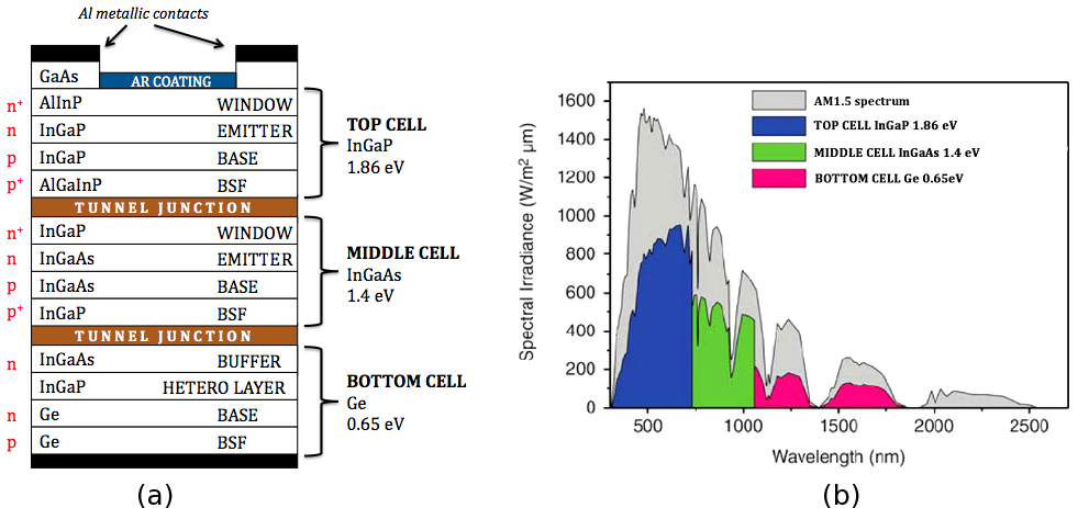
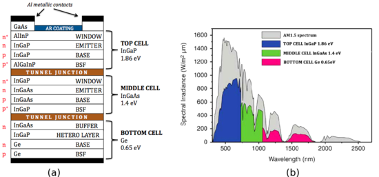 Figure C. (a) The structure of a MJ solar cell. There are six important types of layers: pn junctions, back surface field (BSF) layers, window layers, tunnel junctions, anti-reflective coating and metallic contacts. (b) Graph of spectral irradiance E vs. wavelength λ over the AM1.5 solar spectrum, together with the maximum electricity conversion efficiency for every junction as a function of the wavelength.[9]
Actually producing a tandem cell is not an easy task, largely due to the thinness of the materials and the difficulties extracting the current between the layers. The easy solution is to use two mechanically separate thin film solar cells and then wire them together separately outside the cell. This technique is widely used by amorphous silicon solar cells, Uni-Solar's products use three such layers to reach efficiencies around 9%. Lab examples using more exotic thin-film materials have demonstrated efficiencies over 30%.[11]
The more difficult solution is the "monolithically integrated" cell, where the cell consists of a number of layers that are mechanically and electrically connected. These cells are much more difficult to produce because the electrical characteristics of each layer has to be carefully matched. In particular, the photocurrent generated in each layer needs to be matched, otherwise electrons will be absorbed between layers. This limits their construction to certain materials, best met by the III-V semiconductors.[11]
Material Choice
The choice of materials for each sub-cell is determined by the requirements for lattice-matching, current-matching, and high performance optoelectronic properties.
For optimal growth and resulting crystal quality, the crystal lattice constant a of each material must be closely matched, resulting in lattice-matched devices. This constraint has been relaxed somewhat in recently-developed metamorphic solar cells which contain a small degree of lattice mismatch. However, a greater degree of mismatch or other growth imperfections can lead to crystal defects causing a degradation in electronic properties.
Since each sub-cell is connected electrical in series, the same current flows through each junction. The materials are ordered with decreasing bandgaps, Eg, allowing sub-bandgap light (hc/λ < e·Eg) to transmit to the lower sub-cells. Therefore, suitable bandgaps must be chosen such that the design spectrum will balance the current generation in each of the sub-cells, achieving current matching. Figure C(b) plots spectral irradiance E(λ), which is the source power density at a given wavelength λ. It is plotted together with the maximum conversion efficiency for every junction as a function of the wavelength, which is directly related to the number of photons available for conversion into photocurrent.
Finally, the layers must be electrically optimal for high performance. This necessitates usage of materials with strong absorption coefficients α(λ), high minority carrier lifetimes τminority, and high mobilities µ.[12]
The favorable values in the table below justify the choice of materials typically used for multi-junction solar cells: InGaP for the top sub-cell (Eg = 1.8 - 1.9 eV), InGaAs for the middle sub-cell (Eg = 1.4 eV), and Germanium for the bottom sub-cell (Eg = 0.67 eV). The use of Ge is mainly due to its lattice constant, robustness, low cost, abundance, and ease of production.
Because the different layers are closely lattice-matched, the fabrication of the device typically employs metal-organic chemical vapor deposition (MOCVD). This technique is preferable to the molecular beam epitaxy (MBE) because it ensures high crystal quality and large scale production.[9]
Material Eg, eV a, nm absorption
(λ = 0.8 μm), 1/µmµn, cm²/(V·s) τp, µs Hardness
(Mohs)α, µm/K S, m/s c-Si 1.12 0.5431 0.102 1400 1 7 2.6 0.1–60 InGaP 1.86 0.5451 2 500 – 5 5.3 50 GaAs 1.4 0.5653 0.9 8500 3 4–5 6 50 Ge 0.65 0.5657 3 3900 1000 6 7 1000 InGaAs 1.2 0.5868 30 1200 – – 5.66 100–1000 Structural elements
Metallic contacts
The metallic contacts in aluminium are low-resistivity electrodes that make contact with the semiconductor layer in GaAs. They are positioned on the two sides of the structure but mainly on the backwards face so that shadowing on the lightning surface is reduced.
Anti-reflective coating
Anti-reflective (AR) coating is generally composed of several layers in the case of MJ solar cells. The top AR layer has usually a NaOH surface texturation with several pyramids in order to increase the transmission coefficient T, the trapping of the light in the material (because photons cannot easily get out the MJ structure due to pyramids) and therefore, the path length of photons in the material.[7] On the one hand, the thickness of each AR layer is chosen to get destructive interferences. Therefore, the reflection coefficient R decreases to 1%. In the case of two AR layers L1 (the top layer, usually SiO2) and L2 (usually TiO2), there must be
 to have the same amplitudes for reflected fields and nL1dL1 = 4λmin,nL2dL2 = λmin/4 to have opposite phase for reflected fields.[13] On the other hand, the thickness of each AR layer is also chosen to minimize the reflectance at wavelengths for which the photocurrent is the lowest. Consequently, this maximizes JSC by matching currents of the three subcells.[14]As example, because the current generated by the bottom cell is greater than the currents generated by the other cells, the thickness of AR layers is adjusted so that the infrared (IR) transmission (which corresponds to the bottom cell) is degraded while the ultraviolet transmission (which corresponds to the top cell) is upgraded. Particularly, an AR coating is very important at low wavelengths because, without it, T would be strongly reduced to 70%.
Tunnel junctions
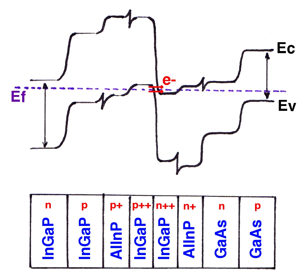
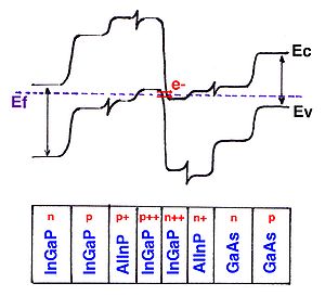 Figure D: Layers and band structure of the tunnel junction. Because the length of the depletion region is narrow and the band gap is high, electrons can tunnel.
The main goal of tunnel junctions is to provide a low electrical resistance and optically low-loss connection between two subcells.[15] Without it, the p-doped region of the top cell would be directly connected with the n-doped region of the middle cell. Hence, a pn junction with opposite direction to the others would appear between the top cell and the middle cell. Consequently, the photovoltage would be lower than if there would be no parasitic diode. In order to decrease this effect, a tunnel junction is used.[16] It is simply a wide band gap, highly doped diode. The high doping reduces the length of the depletion region because
Hence, electrons can easily tunnel through the depletion region. The J-V characteristic of the tunnel junction is very important because it explains why tunnel junctions can be used to have a low electrical resistance connection between two pn junctions. Figure D shows three different regions: the tunneling region, the negative differential resistance region and the thermal diffusion region. The region where electrons can tunnel through the barrier is called the tunneling region. There, the voltage must be low enough so that energy of some electrons who are tunneling is equal to energy states available on the other side of the barrier. Consequently, current density through the tunnel junction is high (with maximum value of JP, the peak current density) and the slope near the origin is therefore steep. Then, the resistance is extremely low and consequently, the voltage too.[17]. This is why tunnel junctions are ideal for connecting two pn junctions without having a voltage drop. When voltage is higher, electrons cannot cross the barrier because energy states are no longer available for electrons. Therefore, the current density decreases and the differential resistance is negative. The last region, called thermal diffusion region, corresponds to the J-V characteristic of the usual diode:
In order to avoid the reduction of the MJ solar cell performances, tunnel junctions must be transparent to wavelengths absorbed by the next photovoltaic cell, the middle cell, i.e. EgTunnel > EgMiddleCell.
Window layer and back-surface field
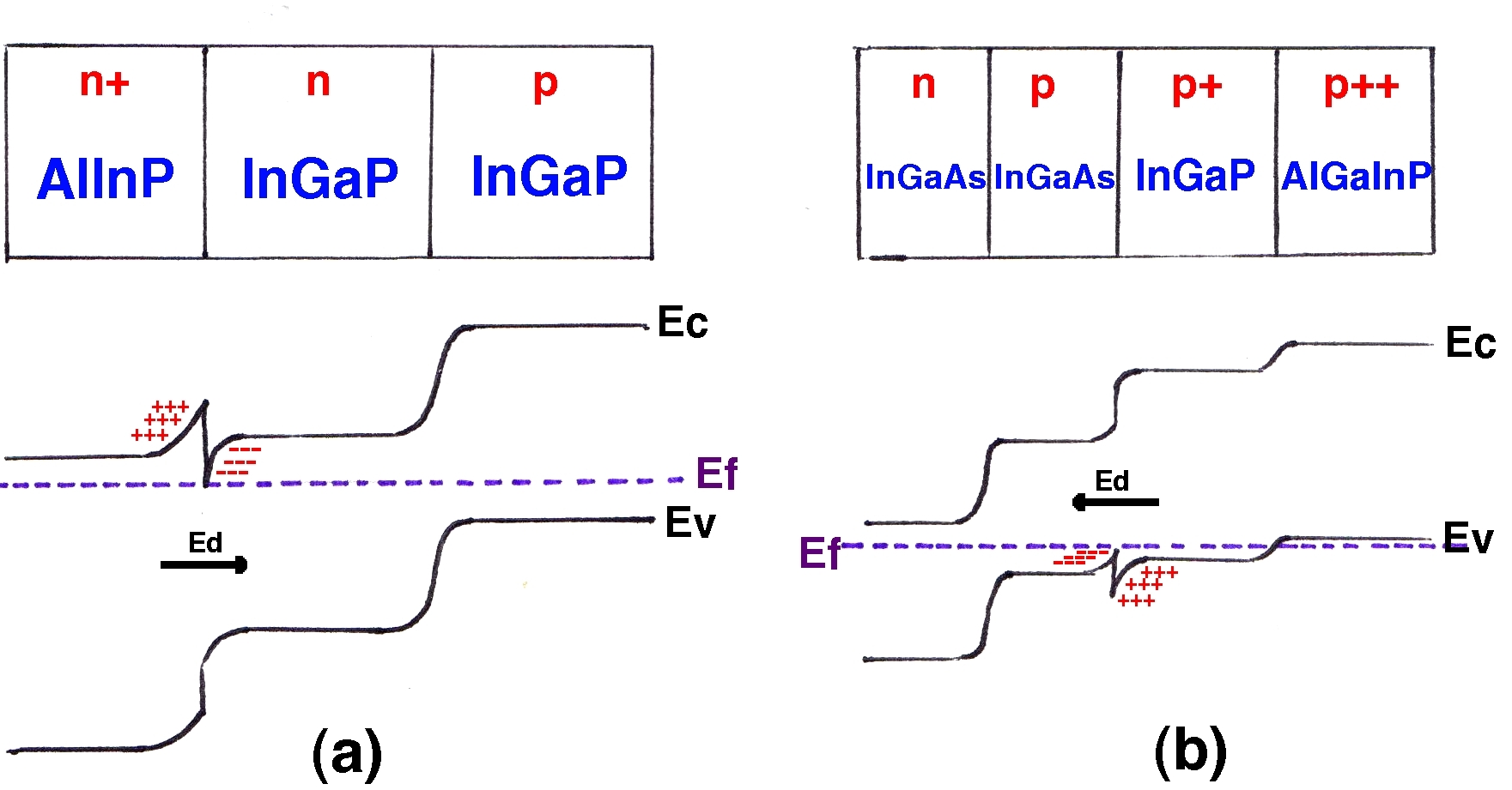
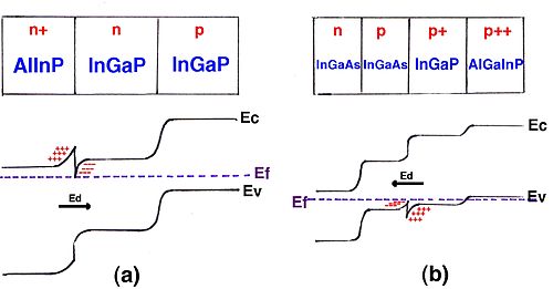 Figure E: (a) Layers and band structure of a window layer. The surface recombination is reduced. (b) Layers and band structure of a BSF layer. The scattering of carriers is reduced.
A window layer is used in order to reduce the surface recombination velocity S. Similarly, a back-surface field (BSF) layer reduces the scattering of carriers towards the tunnel junction. The structure of these two layers is the same: it is a heterojunction which catches electrons (holes). Indeed, despite the electric field Ed, these cannot jump above the barrier formed by the heterojunction because they don't have enough energy, as illustrated in figure E. Hence, electrons (holes) cannot recombine with holes (electrons) and cannot diffuse through the barrier. By the way, window and BSF layers must be transparent to wavelengths absorbed by the next pn junction i.e. EgWindow > EgEmitter and EgBSF > EgEmitter. Furthermore, the lattice constant must be close to the one of InGaP and the layer must be highly doped (n ≥ 1018 cm−3).[18]
J-V characteristic
For maximum efficiency, each subcell should be operated at its optimal J-V parameters, which are not necessarily equal for each subcell. If they are different, the total current through the solar cell is the lowest of the three. By approximation,[19] it results in the same relationship for the short-circuit current of the MJ solar cell: JSC = min (JSC1, JSC2, JSC3) where JSCi(λ) is the short-circuit current density at a given wavelength λ for the subcell i.
Because of the impossibility to obtain JSC1, JSC2, JSC3 directly from the total J-V characteristic, the quantum efficiency QE(λ) is utilized. It measures the ratio between the amount of electron-hole pairs created and the incident photons at a given wavelength λ. Let φi(λ) be the photon flux of corresponding incident light in subcell iandQEi(λ) be the quantum efficiency of the subcell i. By definition, this equates to:[20]
The value of QEi(λ) is obtained by linking it with the absorption coefficientα(λ), i.e. the number of photons absorbed per unit of length by a material. If it is assumed that each photon absorbed by a subcell creates an electron/hole pair (which is a good approximation), this leads to [18]:
 where di is the thickness of the subcell i and
  is the percentage of incident light which is not absorbed by the subcell i.
Similarly, because
 , the following approximation can be used:
  .
.
The values of VOCi are then given by the J-V diode equation:
Materials
The majority of multi-junction cells that have been produced to date use three layers, tuned to blue (on top), yellow and red (on the bottom). These cells require the use of semiconductors that can be tuned to specific frequencies, which has led to most of them being made of gallium arsenide (GaAs) compounds, often germanium for red, GaAs for yellow, and GaInP2 for blue.
Gallium arsenide substrate
Dual junction cells can be made on Gallium arsenide wafers. Alloys of Indium gallium phosphide in the range In.5Ga.5P through In.53Ga.47P serve as the high band gap alloy. This alloy range provides for the ability to have band gaps in the range of 1.92eV to 1.87eV. The lower GaAs junction has a band gap of 1.42eV.[citation needed]
Germanium substrate
Triple junction cells consisting of Indium gallium phosphide, Gallium arsenide or Indium gallium arsenide and Germanium can be fabricated on germanium wafers. Early cells used straight gallium arsenide in the middle junction. Later cells have utilized In0.015Ga0.985As, due to the better lattice match to Ge, resulting in a lower defect density.[citation needed]
Due to the huge band gap difference between GaAs (1.42eV), and Ge (0.66eV), the current match is very poor, with the Ge junction operated significantly current limited.[citation needed]
Current efficiencies for InGaP/GaAs/Ge cells are in the mid 30% range. Lab cells using additional junctions between the GaAs and Ge junction have demonstrated efficiencies above 40%.
Indium phosphide substrate
Indium phosphide may be used as a substrate to fabricate cells with band gaps between 1.35eV and 0.74eV. Indium Phosphide has a band gap of 1.35eV. Indium gallium arsenide(In0.53Ga0.47As) is lattice matched to Indium Phosphide with a band gap of 0.74eV. A quaternary alloy of Indium gallium arsenide phosphide can be lattice matched for any band gap in between the two.[citation needed]
Indium phosphide-based cells have the potential to work in tandem with gallium arsenide cells. The two cells can be optically connected in series (with the InP cell below the GaAs cell), or in parallel through the use of spectra splitting using a Dichroic filter.[citation needed]
Performance improvements
Structure
All MJ photovoltaic cells use III-V semiconductor materials. GaAsSb-based heterojunction tunnel diodes, instead of conventional InGaP highly doped tunnel diodes described above, have a lower tunneling distance. Indeed, in the heterostructure formed by GaAsSb and InGaAs, the valence band of GaAsSb is higher than the valence band of the adjoining p-doped layer.[16] Consequently, the tunneling distance dtunnel is reduced and so the tunneling current, which exponentially depends of dtunnel, is increased. Hence, the voltage is lower than that of the InGaP tunnel junction. GaAsSb heterojunction tunnel diodes offer other advantages. The same current can be achieved by using a lower doping. [21]Secondly, because the lattice constant is larger for GaAsSb than Ge, one can use a wider range of materials for the bottom cell because more materials are lattice-matched to GaAsSb than to Ge.[16]
Chemical components can be added to some layers. Adding about one percent of Indium in each layer better matches lattice constants of the different layers.[22] Without it, there is about 0.08 percent of mismatching between layers, which inhibits performance. Adding aluminium to the top cell increases its band gap to 1.96 eV,[22] covering a larger part of the solar spectrum and obtain a higher open-circuit voltage VOC.
The theoretical efficiency of MJ solar cells is 86.8% for an infinite number of pn junctions,[9] implying that more junctions increase efficiency. The maximum theoretical efficiency is 37, 50, 56, 72% for 1, 2, 3, 36 pn junctions, respectively, with the number of junctions increasing exponentially to achieve equal effiency increments.[18] The exponential relationship implies that as the cell approaches the limit of efficiency, the increase cost and complexity grow rapidly. Decreasing the thickness of the top cell increases the transmission coefficient T.[18]
Finally, an InGaP hetero-layer between the p-Ge layer and the InGaAs layer can be added in order to create automatically the n-Ge layer by scattering during MOCVD growth and increase significantly the quantum efficiency QE(λ) of the bottom cell.[22] InGaP is advantageous because of its high scattering coefficient and low solubility in Ge.
Spectral variations
Solar spectrum at the Earth surface changes constantly depending on the weather and sun position. This results in the variation of φ(λ), QE(λ), α(λ) and thus the short-circuit currents JSCi. As a result, the current densities Ji are not necessarily matched and the total current becomes lower. These variations can be quantified using the average photon energy (APE) which is the ratio between the spectral irradiance G(λ) (the power density of the light source in a specific wavelength λ) and the total photon flux density. It can be shown that a high (low) value for APE means low (high) wavelengths spectral conditions and higher (lower) efficiencies.[23] Thus APE is a good indicator for quantifying the effects of the solar spectrum variations on performances and has the added advantage of being independent of the device structure and the absorption profile of the device.[23]
Use of light concentrators
Light concentrators increase efficiencies and reduce the cost/efficiency ratio. The two types of light concentrators are refractive lenses like Fresnel lenses and reflective dishes. Thanks to these devices, light arriving on a large surface can be concentrated on a smaller cell. The intensity concentration ratio (or “suns”) is the average intensity of the focused light divided by 0.1 W/m². If its value is X then the MJ current becomes X higher under concentrated illumination.[24][25]
Using concentrations on the order of 500 to 1000, meaning that a 1 cm² cell can use the light collected from 0.1 m² (as 1 m2 equal 10000 cm2), produces the highest efficiencies seen to date. Three-layer cells are fundamentally limited to 63%, but existing commercial prototypes have already demonstrated over 40%.[26][27] These cells capture about 2/3 of their theoretical maximum performance, so assuming the same is true for a non-concentrated version of the same design, one might expect a three-layer cell of 30% efficiency. This is not enough of an advantage over traditional silicon designs to make up for their extra production costs. For this reason, almost all multi-junction cell research for terrestrial use is dedicated to concentrator systems, normally using mirrors or fresnel lenses.
Using a concentrator also has the added benefit that the number of cells needed to cover a given amount of ground area is greatly reduced. A conventional system covering 1 m² would require 625 16 cm² cells, but for a concentrator system only a single cell is needed, along with a concentrator. The argument for concentrated Multi-junction cells has been that the high cost of the cells themselves would be more than offset by the reduction in total number of cells. However, the downside of the concentrator approach is that efficiency drops off very quickly under lower lighting conditions. In order to maximize its advantage over traditional cells and thus be cost competitive, the concentrator system has to track the sun as it moves to keep the light focused on the cell and maintain maximum efficiency as long as possible. This requires an expensive solar tracker system, and offsets the potential advantages offered by multi-junction cells.
Fabrication
Multi-junction cells are expensive to produce, using techniques similar to semiconductor device fabrication, usually metalorganic vapour phase epitaxy but on "chip" sizes on the order of centimeters. In cases where outright performance is the only consideration, these cells have become common, they are widely used in satellite applications for instance, where the power-to-weight ratio overwhelms practically every other cost.
Comparison with other technologies
There are four main categories of photovoltaic cells: c-Si solar cells, thin film solar cells, MJ solar cells and new technologies (including organic solar cells).
Technology η (%) VOC (V) ISC (A) W/m² t (µm) u c-Si 24.7 0.5 0.8 63 100 p c-Si 20.3 0.615 8.35 211 200 a-Si 11.1 6.3 0.0089 33 1 CdTe 16.5 0.86 0.029 – 5 CIGS 19.5 – – – 1 MJ 40.7 2.6 1.81 476 140 MJ solar cells and other photovoltaic devices have significant differences (see the table above). Physically, the main property of a MJ solar cell is having more than one pn junction in order to catch a larger photon energy spectrum while the main property of the thin film solar cell is to use thin films instead of thick layers in order to decrease the cost efficiency ratio. As of 2010, MJ solar panels are more expensive than others. These differences imply different applications: MJ solar cells are preferred in space and c-Si solar cells for terrestrian applications.
The efficiencies of solar cells and Si solar technology are relatively stable, while the efficiency of solar modules and multi-junction technology are progressing.
Measurements on MJ solar cells are usually made in laboratory, using light concentrators (this is often not the case for the other cells) and under standard test conditions (STCs). STCs prescribe, for terrestrial applications, the AM1.5 spectrum as the reference. This air mass (AM) corresponds to a fixed position of the sun in the sky of 48° and a fixed power of 833 W/m². Therefore, spectral variations of incident light and environmental parameters are not taken into account under STC.[28]
Consequently, performance of MJ solar cells in terrestrial environment is inferior to that achieved in laboratory. Moreover, MJ solar cells are designed such that currents are matched under STC, but not necessarily under field conditions. One can use QE(λ) to compare performances of different technologies, but QE(λ) contains no information on the matching of currents of subcells. An important comparison point is rather the output power per unit area generated with the same incident light.
Applications
As of 2010, the cost of MJ solar cells was too high to allow use outside of specialized applications. The high cost is mainly due to the complex structure and the high price of materials. Nevertheless, with light concentrators under illumination of at least 400 suns, MJ solar panels become practical.[18]
MJ cells are currently being utilized in the Mars rover missions.[29]
The environment in space is quite different. Because there is no atmosphere, the solar spectrum is different (AM0). The cells have a poor current match due to a greater photon flux of photons above 1.87eV vs. those between 1.87eV and 1.42eV. This results in too little current in the GaAs junction, and hampers the overall efficiency since the InGaP junction operates below MPP current and the GaAs junction operates above MPP current. To improve current match, the InGaP layer is intentionally thinned to allow additional photons to penetrate to the lower GaAs layer.[citation needed]
In terrestrial concentrating applications, the scatter of blue light by the atmosphere reduces the photon flux above 1.87eV, better balancing the junction currents.Radiation particles that are no longer filtered can cause damage the cell. There are two kinds of damage: ionisation and atomic displacement.[30] Still, MJ cells offer higher radiation resistance, higher efficiency and a lower temperature coefficient.[18]
References
- ^ http://www.nsinnovations.com.au/news/solar_cell_record.html
- ^ Spire pushes solar cell record to 42.3%. Optics.org. Retrieved on 2011-01-19.
- ^ "ZTJ Space Solar Cell", emcore
- ^ "Concentrating Photovoltaic Technology", NREL
- ^ CPV World Map 2011
- ^ "Uni-Solar Energy Production", Uni-Solar
- ^ a b R.Delamare, O.Bulteel, D.Flandre, Conversion lumière/électricité: notions fondamentales et exemples de recherche
- ^ "Basic Photovoltaic Principles and Methods", Technical Information Office, Solar Energy Research Institute (1982)
- ^ a b c d N.V.Yastrebova (2007). High-efficiency multi-junction solar cells: current status and future potential. http://sunlab.site.uottawa.ca/pdf/whitepapers/HiEfficMjSc-CurrStatus&FuturePotential.pdf.
- ^ Green, M.A. (2003). Third Generation Photovoltaics. Springer-Verlag. ISBN 10 3-540-26562-7.
- ^ a b c "Tandem solar cells"
- ^ Miles, R (2006). "Photovoltaic solar cells: Choice of materials and production methods". Vacuum 80 (10): 1090. doi:10.1016/j.vacuum.2006.01.006.
- ^ Strehlke, S; Bastide, S; Guillet, J; Levyclement, C (2000). "Design of porous silicon antireflection coatings for silicon solar cells". Materials Science and Engineering B 69-70: 81. doi:10.1016/S0921-5107(99)00272-X.
- ^ Daniel J.Aiken (2000). "Antireflection coating design for multi-junction, series interconnected solar cells". Progress in Photovoltaics: Research and Applications 8 (6): 563–570. doi:10.1002/1099-159X(200011/12)8:6<563::AID-PIP327>3.0.CO;2–8. http://photovoltaics.sandia.gov/docs/PDF/aikencell.pdf.
- ^ Yamaguchi, M; Takamoto, T; Araki, K (2006). "Super high-efficiency multi-junction and concentrator solar cells". Solar Energy Materials and Solar Cells 90 (18–19): 3068. doi:10.1016/j.solmat.2006.06.028.
- ^ a b c J.F.Klem, S.Park, J.C.Zolper, Semiconductor tunnel junction with enhancement layer, U.S. Patent 5,679,963(1997)
- ^ J.F.Wheeldonet al. (2009). AlGaAs Tunnel Junction for high efficiency multi-junction solar cells: simulation and measurement of temperature-dependent operation. http://sunlab.site.uottawa.ca/pdf/conferences/PVSC2009_JWheeldon_AlGaAsTjHiEfficMjSc-Sim&MeasTDep.pdf.
- ^ a b c d e f Luque & Hegedus 2003, p. 390 ff
- ^ Peharz, G.; Siefer, G.; Bett, A.W. (2009). "A simple method for quantifying spectral impacts on multi-junction solar cells". Solar Energy 83 (9): 1588. doi:10.1016/j.solener.2009.05.009.
- ^ Liu, Lei; Chen, Nuofu; Bai, Yiming; Cui, Ming; Zhang, Han; Gao, Fubao; Yin, Zhigang; Zhang, Xingwang (2008). "Quantum efficiency and temperature coefficients of GaInP/GaAs dual-junction solar cell". Science in China Series E: Technological Sciences 52 (5): 1176. doi:10.1007/s11431-008-0203-9.
- ^ J.C. Zolper et al. (1994). GaAsSb-based heterojunction tunnel diodes for tandem solar cell interconnects. 2. pp. 1843. doi:10.1109/WCPEC.1994.520724. http://www.osti.gov/bridge/servlets/purl/10107906-3FIrKs/webviewable/.
- ^ a b c Yamaguchi, M; Takamoto, T; Araki, K; Ekinsdaukes, N (2005). "Multi-junction III–V solar cells: current status and future potential". Solar Energy 79 (1): 78. doi:10.1016/j.solener.2004.09.018.
- ^ a b Impact of spectral effects on the electrical parameters of multijunction amorphous silicon cells. doi:10.1109/WCPEC.2003.1306273. http://hdl.handle.net/2134/8216.
- ^ Luque & Hegedus 2003, pp. 61 ff
- ^ Luque & Hegedus 2003, pp. 449 ff
- ^ Michael Kanellos, "Solar cell breaks efficiency record", CNET News, 6 December 2006
- ^ "NREL Solar Cell Sets World Efficiency Record at 40.8 Percent", National Renewable Energy Laboratory, 13 August 2008
- ^ Albuflasa, H; Gottschalg, R; Betts, T (2007). "Modeling the effect of varying spectra on multi junction A-SI solar cells". Desalination 209 (1–3): 78. doi:10.1016/j.desal.2007.04.012.
- ^ D. Crisp, , a, A. Pathareb and R. C. Ewell (2004). "The performance of gallium arsenide/germanium solar cells at the Martian surface". Progress in Photovoltaics: Research and Applications 54 (2): 83–101. doi:10.1016/S0094-5765(02)00287-4.
- ^ Luque & Hegedus 2003, pp. 414 ff
Bibliography
- Luque, Antonio; Hegedus, eds (2003). Handbook of Photovoltaic Science and Engineering. John Wiley and Sons. ISBN 0471491969. http://books.google.com/books?id=u-bCMhl_JjQC&pg=PT390.
See also
- List of semiconductor materials
- Organic photovoltaic cell
- p-i-n and n-i-p
Photovoltaics Concepts - Photoelectric effect
- Photovoltaics
- History of photovoltaics
- Timeline of solar cells
- Solar insolation
- Solar constant
- Solar cell efficiency
- Third generation photovoltaic cell
- Solar cell research
- Quantum efficiency of a solar cell
- Cadmium telluride
- Thermophotovoltaic
- Polycrystalline silicon photovoltaics
- Thermodynamic efficiency limit
- Sun-free photovoltaics
- Polarizing organic photovoltaics
Photovoltaic system Solar cells- Solar cell
- Solar panel
- Thin film solar cell
- Polymer solar cell
- Nanocrystal solar cell
- Organic solar cell
- Quantum dot solar cell
- Hybrid solar cell
- Plasmonic solar cell
- Carbon nanotubes in photovoltaics
- Dye-sensitized solar cell
- Cadmium telluride photovoltaics
- Copper indium gallium selenide solar cells
- Multijunction photovoltaic cell
- Printed solar panel
System components- Solar charge controller
- Solar inverter
- Solar micro-inverter
- Solar cable
- Solar combiner box
- Photovoltaic mounting system
- Maximum power point tracker
- Solar tracker
- Solar shingles
- Solar mirror
System concepts- Perturb and observe method
- Incremental conductance method
- Constant voltage method
- Fill factor
- Concentrated photovoltaics
- Photovoltaic thermal hybrid solar collector
- Space-based solar power
- Watt-peak
Applications Appliances- Solar-powered refrigerator
- Solar air conditioning
- Solar lamp
- Solar charger
- Solar backpack
- Solar tree
- Solar-powered pump
- Solar-powered watch
- Solar Tuki
- Photovoltaic keyboard
- Solar road stud
- Solar cell phone charger
- Solar notebook
- Solar powered calculator
- Solar powered fountain
- Solar powered radio
- Solar powered flashlight
- Solar fan
- Solar street light
- Solar traffic light
Land transport- Solar vehicle
- Solar car
- Solar roadway
- Solar golf cart
- The Quiet Achiever
- Sunmobile
Air transport- Electric aircraft
- Mauro Solar Riser
- Solar panels on spacecraft
- Solar-Powered Aircraft Developments Solar One
- Gossamer Penguin
- Qinetiq Zephyr
- Solar Challenger
Water transportSolar vehicle racing- Solar car racing
- List of solar car teams
- Solar challenge
- Solar Cup
- Blue Sky Solar Racing
- Frisian Solar Challenge
- UC Solar Team
- Solar Splash
- South African Solar Challenge
- Tour de Sol
- World Solar Challenge
- Hunt-Winston School Solar Car Challenge
- North American Solar Challenge
- Victorian Model Solar Vehicle Challenge
Generation systems - Solar Energy Generating Systems
- Stand-alone photovoltaic power system
- Grid-connected photovoltaic power system
- Rooftop photovoltaic power station
- Topaz Solar Farm
- Solar Ark
- Solar Umbrella house
- Erlasee Solar Park
- Guadarranque solar power plant
- Pocking Solar Park
- Copper Mountain Solar Facility
- Wyandot Solar Facility
- Köthen Solar Park
- Building-integrated photovoltaics
- Moura Photovoltaic Power Station
- Nevada Solar One
- Beneixama photovoltaic power plant
- Gottelborn Solar Park
- Darro Solar Park
- Olmedilla Photovoltaic Park
- Blythe Photovoltaic Power Plant
- Strasskirchen Solar Park
- Puertollano Photovoltaic Park
- Alamosa photovoltaic power plant
By countryList of countries by photovoltaics productionPV companies Categories:- Solar cells
- Energy conversion
- Semiconductor devices
- Electronics terms


Wikimedia Foundation. 2010.