- Delta-sigma modulation
-
Delta-sigma (ΔΣ; or sigma-delta, ΣΔ) modulation is a method for encoding high-resolution or analog signals into lower-resolution digital signals. The conversion is done using error feedback, where the difference between the two signals is measured and used to improve the conversion. The low-resolution signal typically changes more quickly than the high-resolution signal and it can be filtered to recover the high-resolution signal with little or no loss of fidelity. This technique has found increasing use in modern electronic components such as analog-to-digital converters (ADCs) and digital-to-analog converters (DACs), frequency synthesizers, switched-mode power supplies and motor controllers.
A very popular application of delta-sigma conversion is in audio applications where a digital audio signal, as from an MP3 player, is converted into the analog audio signal which will be amplified and output by speakers or headphones. Because most of the modulator is a digital circuit, it is cheap to construct. Since the output of this modulator typically has only two levels, the generation of the analog output signal is power efficient. Further, because the modulator's output signal changes much faster than the desired audio signal, it can be heavily filtered and the resulting analog signal has high enough fidelity for use in professional applications.
Low cost, low power, and high fidelity make delta-sigma modulators very popular.
Contents
Motivation
Why convert an analog signal into a stream of pulses?
In brief, because it is very easy to regenerate pulses at the receiver into the ideal form transmitted. The only part of the transmitted waveform required at the receiver is the time at which the pulse occurred. Given the timing information the transmitted waveform can be reconstructed electronically with great precision. In contrast, without conversion to a pulse stream but simply transmitting the analog signal directly, all noise in the system is added to the wanted analog signal quickly rendering it useless.
Each pulse is made up of a step up followed after a short interval by a step down. It is possible, even in the presence of electronic noise, to recover the timing of these steps and from that regenerate the transmitted pulse stream almost noiselessly. Then the accuracy of the transmission process reduces to the accuracy with which the transmitted pulse stream represents the input waveform.
There are several methods available to the specialist for quantifying the distortions introduced, all of which are technical, mathematical and are assumed to be of no great interest or value to the layman and so he may safely skip the mathematics. All the layman needs to know is that the specialists have determined that the distortions are within acceptable limits and may even have a value in reducing unwanted aspects of the original signal.
Why delta-sigma modulation?
Delta-sigma modulation converts the analog voltage into a pulse frequency and is alternative known as Pulse Density modulation or Pulse Frequency modulation. In general frequency may vary smoothly in infinitesimal steps as may voltage and both may serve as an analog of an infinitesimally varying physical variable such as acoustic pressure, light intensity etc. so the substitution of frequency for voltage is entirely natural and carries in its train the transmission advantages of a pulse stream. The different names for the modulation method are the result of pulse frequency modulation by different electronic implementations which all produce similar transmitted waveforms.
Why use delta-sigma modulation on a CD?
A CD works by optically reading pits formed on the CD. This reading process does not necessarily produce well formed pulses but the pulses may be electronically reformed so that only the presence or absence of a pit need be detected. This gives the advantage of pulse modulation methods in general in that amplitude variation of the recovered pulses is compensated by pulse regeneration. In the case of CD,s the resultant pulses are interpreted by a method known as PCM. This method uses an analog to digital converter (ADC). The ADC can be implemented using the method described below. Using an ADC the mean value of samples of the analog signal, possibly enhanced by signal processing techniques, taken over a small interval, are expressed numerically and these numbers are recorded digitally by means of the pits on the CD. Alternatively, SACD is a method used on some CD,s. In this method the quasi-instantaneous value of the analog signal is represented by the duty cycle of the pulse stream,ie. the quasi-instantaneous ratio of the duration of high pulse level (the mark) to the period, where the period is sum of the duration of low pulse level (the space) and the duration of the mark. Again, only timing of the transition is important as the pulse stream waveform can be restored from the timing. Also, the duty cycle may be varied infinitesimally and so is a natural candidate for the representation of an analog signal.
Why the delta-sigma analog to digital conversion?
The ADC accurately converts the mean of an analog voltage into the mean of an analog pulse frequency and counts the pulses in an accurately known interval so that the pulse count divided by the interval gives an accurate digital representation of the mean analog voltage during the interval. This interval can be chosen to give any desired resolution or accuracy and the method is cheaply produced by modern methods. Thus it is popular and widely used. ΣΔ is the mathematical symbol for the summation of delta pulses and is read sigma-delta.
Analog to digital conversion
Description
The analog to digital converter, ADC, generates a pulse stream in which the frequency of pulses in the stream is proportional to the analog voltage input, v, so that the frequency,
 where k is a constant for the particular implementation.
A counter sums the number of pulses that occur in a predetermined period, P so that the sum, Σ, is
 .
. is chosen so that a digital display of the count, Σ, is a display of v with a predetermined scaling factor. Because P may take any designed value it may be made large enough to give any desired resolution or accuracy.
Each pulse of the pulse stream has a known, constant amplitude V and duration
 , and thus has a known integral
  but variable separating interval.
In a formal analysis an impulse such as integral
is treated as the Dirac δ (delta) function and is specified by the step produced on integration. Here we indicate that step as  .
.The interval between pulses, p, is determined by a feedback loop arranged so that
 .
.The action of the feedback loop is to monitor the integral of v and when that integral has incremented by Δ, which is indicated by the integral waveform crossing a threshold, then subtracting Δ from the integral of v so that the combined waveform sawtooths between the threshold and ( threshold - Δ ). At each step a pulse is added to the pulse stream.
Between impulses the slope of the integral is proportional to
 . Whence
  .
.It is the pulse stream which is transmitted for delta-sigma modulation but the pulses are counted to form sigma in the case of analogue to digital conversion.
Analysis
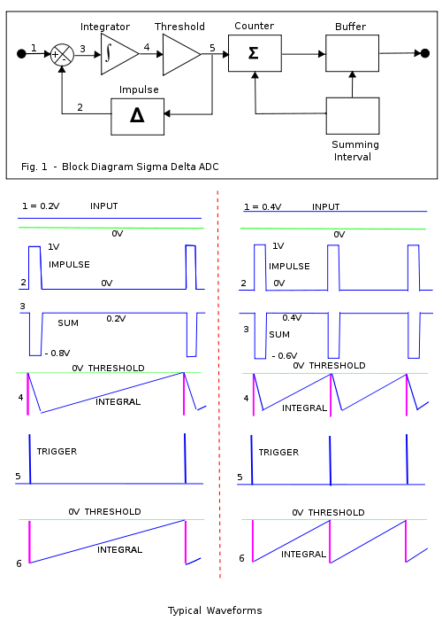 Fig. 1: Block diagram and waveforms for a sigma delta ADC.
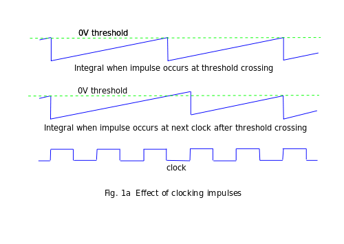 Fig. 1a: Effect of clocking impulses
Shown below the block diagram illustrated in Fig. 1 are waveforms at points designated by numbers 1 to 5 for an input of 0.2 volts on the left and 0.4 volts on the right.
In most practical applications the summing interval is large compared with the impulse duration and for signals which are a significant fraction of full scale the variable separating interval is also small compared with the summing interval. The Nyquist–Shannon sampling theorem requires two samples to render a varying input signal. The samples appropriate to this criterion are two successive Σ counts taken in two successive summing intervals. The summing interval, which must accommodate a large count in order to achieve adequate precision, is inevitably long so that the converter can only render relatively low frequencies. Hence it is convenient and fair to represent the input voltage (1) as constant over a few impulses.
Consider first the waveforms on the left.
1 is the input and for this short interval is constant at 0.2 V. The stream of delta impulses is shown at 2 and the difference between 1 and 2 is shown at 3. This difference is integrated to produce the waveform 4. The threshold detector generates a pulse 5 which starts as the waveform 4 crosses the threshold and is sustained until the waveform 4 falls below the threshold. Within the loop 5 triggers the impulse generator and external to the loop increments the counter. The summing interval is a prefixed time and at its expiry the count is strobed into the buffer and the counter reset.
It is necessary that the ratio between the impulse interval and the summing interval is equal to the maximum (full scale) count. It is then possible for the impulse duration and the summing interval to be defined by the same clock with a suitable arrangement of logic and counters. This has the advantage that neither interval has to be defined with absolute precision as only the ratio is important. Then to achieve overall accuracy it is only necessary that the amplitude of the impulse be accurately defined.
On the right the input is now 0.4 V and the sum during the impulse is −0.6 V as opposed to −0.8 V on the left. Thus the negative slope during the impulse is lower on the right than on the left.
Also the sum is 0.4 V on the right during the interval as opposed to 0.2 V on the left. Thus the positive slope outside the impulse is higher on the right than on the left.
The resultant effect is that the integral (4) crosses the threshold more quickly on the right than on the left. A full analysis would show that in fact the interval between threshold crossings on the right is half that on the left. Thus the frequency of impulses is doubled. Hence the count increments at twice the speed on the right to that on the left which is consistent with the input voltage being doubled.
Construction of the waveforms illustrated at (4) is aided by concepts associated with the Dirac delta function in that all impulses of the same strength produce the same step when integrated, by definition. Then (4) is constructed using an intermediate step (6) in which each integrated impulse is represented by a step of the assigned strength which decays to zero at the rate determined by the input voltage. The effect of the finite duration of the impulse is constructed in (4) by drawing a line from the base of the impulse step at zero volts to intersect the decay line from (6) at the full duration of the impulse.
As stated, Fig. 1 is a simplified block diagram of the delta-sigma ADC in which the various functional elements have been separated out for individual treatment and which tries to be independent of any particular implementation. Many particular implementations seek to define the impulse duration and the summing interval from the same clock as discussed above but in such a way that the start of the impulse is delayed until the next occurrence of the appropriate clock pulse boundary. The effect of this delay is illustrated in Fig. 1a for a sequence of impulses which occur at a nominal 2.5 clock intervals, firstly for impulses generated immediately the threshold is crossed as previously discussed and secondly for impulses delayed by the clock. The effect of the delay is firstly that the ramp continues until the onset of the impulse, secondly that the impulse produces a fixed amplitude step so that the integral retains the excess it acquired during the impulse delay and so the ramp restarts from a higher point and is now on the same locus as the unclocked integral. The effect is that, for this example, the undelayed impulses will occur at clock points 0, 2.5, 5, 7.5, 10, etc. and the clocked impulses will occur at 0, 3, 5, 8, 10, etc. The maximum error that can occur due to clocking is marginally less than one count. Although the Sigma-Delta converter is generally implemented using a common clock to define the impulse duration and the summing interval it is not absolutely necessary and an implementation in which the durations are independently defined avoids one source of noise, the noise generated by waiting for the next common clock boundary. Where noise is a primary consideration that overrides the need for absolute amplitude accuracy; e.g., in bandwidth limited signal transmission, separately defined intervals may be implemented.
Practical Implementation
 Fig. 1b: circuit diagram
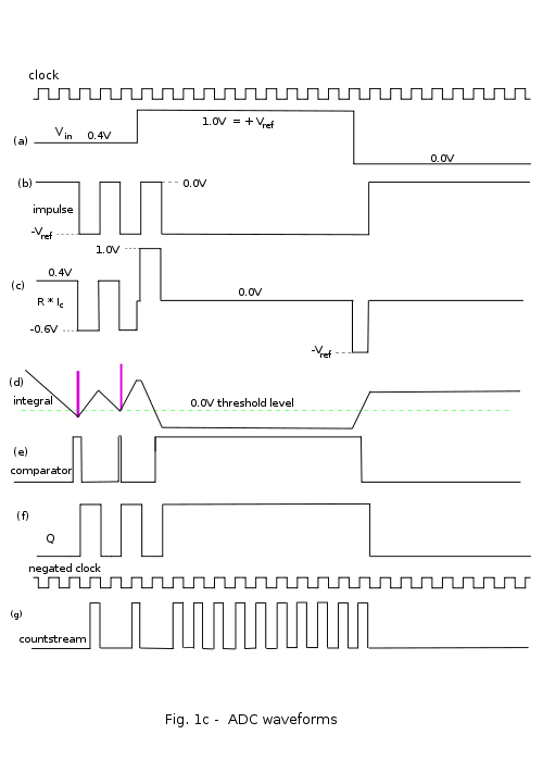 Fig. 1c: ADC waveforms
A circuit diagram for a practical implementation is illustrated, Fig 1b and the associated waveforms Fig. 1c. A scrap view of an alternative front end is shown in Fig. 1b which has the advantage that the voltage at the switch terminals are relatively constant and close to 0.0 V. Also the current generated through R by −Vref is constant at −Vref/R so that much less noise is radiated to adjacent parts of the circuit. Then this would be the preferred front end in practice but, in order to show the impulse as a voltage pulse so as to be consistent with previous discussion, the front end given here, which is an electrical equivalent, is used.
From the top of Fig 1c the waveforms, labelled as they are on the circuit diagram, are:-
The clock.
(a) Vin. This is shown as varying from 0.4 V initially to 1.0 V and then to zero volts to show the effect on the feedback loop.
(b) The impulse waveform. It will be discovered how this acquires its form as we traverse the feedback loop.
(c) The current into the capacitor, Ic, is the linear sum of the impulse voltage upon R and Vin upon R. To show this sum as a voltage the product R × Ic is plotted. The input impedance of the amplifier is regarded as so high that the current drawn by the input is neglected.
(d) The negated integral of Ic. This negation is standard for the op. amp. implementation of an integrator and comes about because the current into the capacitor at the amplifier input is the current out of the capacitor at the amplifier output and the voltage is the integral of the current divided by the capacitance of C.
(e) The comparator output. The comparator is a very high gain amplifier with its plus input terminal connected for reference to 0.0 V. Whenever the negative input terminal is taken negative with respect the positive terminal of the amplifier the output saturates positive and conversely negative saturation for positive input. Thus the output saturates positive whenever the integral (d) goes below the 0 V reference level and remains there until (d) goes positive with respect to the reference level.
(f) The impulse timer is a D type positive edge triggered flip flop. Input information applied at D is transferred to Q on the occurrence of the positive edge of the clock pulse. thus when the comparator output (e) is positive Q goes positive or remains positive at the next positive clock edge. Similarly, when (e) is negative Q goes negative at the next positive clock edge. Q controls the electronic switch to generate the current impulse into the integrator. Examination of the waveform (e) during the initial period illustrated, when Vin is 0.4 V, shows (e) crossing the threshold well before the trigger edge (positive edge of the clock pulse) so that there is an appreciable delay before the impulse starts. After the start of the impulse there is further delay while (e) climbs back past the threshold. During this time the comparator output remains high but goes low before the next trigger edge. At that next trigger edge the impulse timer goes low to follow the comparator. Thus the clock determines the duration of the impulse. For the next impulse the threshold is crossed immediately before the trigger edge and so the comparator is only briefly positive. Vin (a) goes to full scale, +Vref, shortly before the end of the next impulse. For the remainder of that impulse the capacitor current (c) goes to zero and hence the integrator slope briefly goes to zero. Following this impulse the full scale positive current is flowing (c) and the integrator sinks at its maximum rate and so crosses the threshold well before the next trigger edge. At that edge the impulse starts and the Vin current is now matched by the reference current so that the net capacitor current (c) is zero. Then the integration now has zero slope and remains at the negative value it had at the start of the impulse. This has the effect that the impulse current remains switched on because Q is stuck positive because the comparator is stuck positive at every trigger edge. This is consistent with contiguous, butting impulses which is required at full scale input.
Eventually Vin (a) goes to zero which means that the current sum (c) goes fully negative and the integral ramps up. It shortly thereafter crosses the threshold and this in turn is followed by Q, thus switching the impulse current off. The capacitor current (c) is now zero and so the integral slope is zero, remaining constant at the value it had acquired at the end of the impulse.
(g) The countstream is generated by gating the negated clock with Q to produce this waveform. Thereafter the summing interval, sigma count and buffered count are produced using appropriate counters and registers. The Vin waveform is approximated by passing the countstream (g) into a low pass filter, however it suffers from the defect discussed in the context of Fig. 1a. One possibility for reducing this error is to halve the feedback pulse length to half a clock period and double its amplitude by halving the impulse defining resistor thus producing an impulse of the same strength but one which never butts onto its adjacent impulses. Then there will be a threshold crossing for every impulse. In this arrangement a monostable flip flop triggered by the comparator at the threshold crossing will closely follow the threshold crossings and thus eliminate one source of error, both in the ADC and the sigma delta modulator.
Remarks
In this section we have mainly dealt with the analogue to digital converter as a stand alone function which achieves astonishing accuracy with what is now a very simple and cheap architecture. Initially the Delta-Sigma configuration was devised by INOSE et al. to solve problems in the accurate transmission of analog signals. In that application it was the pulse stream that was transmitted and the original analog signal recovered with a low pass filter after the received pulses had been reformed. This low pass filter performed the summation function associated with Σ. The highly mathematical treatment of transmission errors was introduced by them and is appropriate when applied to the pulse stream but these errors are lost in the accumulation process associated with Σ to be replaced with the errors associated with the mean of means when discussing the ADC. For those uncomfortable with this assertion consider this.
It is well known that by Fourier analysis techniques the incoming waveform can be represented over the summing interval by the sum of a constant plus a fundamental and harmonics each of which has an exact integer number of cycles over the sampling period. It is also well known that the integral of a sine wave or cosine wave over one or more full cycles is zero. Then the integral of the incoming waveform over the summing interval reduces to the integral of the constant and when that integral is divided by the summing interval it becomes the mean over that interval. The interval between pulses is proportional to the inverse of the mean of the input voltage during that interval and thus over that interval, ts, is a sample of the mean of the input voltage proportional to V/ts. Thus the average of the input voltage over the summing period is VΣ/N and is the mean of means and so subject to little variance.
Unfortunately the analysis for the transmitted pulse stream has, in many cases, been carried over, uncritically, to the ADC.
It was indicated in section 1.3 Analysis that the effect of constraining a pulse to only occur on clock boundaries is to introduce noise, that generated by waiting for the next clock boundary. This will have its most deleterious effect on the high frequency components of a complex signal. Whilst the case has been made for clocking in the ADC environment, where it removes one source of error, namely the ratio between the impulse duration and the summing interval, it is deeply unclear what useful purpose clocking serves in a transmission environment since it is a source of both noise and complexity.
A very accurate transmission system with constant sampling rate may be formed using the full arrangement shown here by transmitting the samples from the buffer protected with redundancy error correction. In this case there will be a trade off between bandwidth and N, the size of the buffer. The signal recovery system will require redundancy error checking, digital to analog conversion,and sample and hold circuitry. A possible further enhancement is to include some form of slope regeneration.This amounts to PCM (pulse code modulation) with digitization performed by a sigma-delta ADC.
The above description shows why the impulse is called delta. The integral of an impulse is a step. A one bit DAC may be expected to produce a step and so must be a conflation of an impulse and an integration. The analysis which treats the impulse as the output of a 1-bit DAC hides the structure behind the name (sigma delta) and cause confusion and difficulty interpreting the name as an indication of function. This analysis is very widespread but is deprecated.
A modern alternative method for generating voltage to frequency conversion is discussed in synchronous voltage to frequency converter (SVFC) which may be followed by a counter to produce a digital representation in a similar manner to that described above.[1]
Digital to analog conversion
Discussion
Delta-sigma modulators are often used in digital to analog converters (DACs). In general, a DAC converts a digital number representing some analog value into that analog value. For example, the analog voltage level into a speaker may be represented as a 20 bit digital number, and the DAC converts that number into the desired voltage. To actually drive a load (like a speaker) a DAC is usually connected to or integrated with an electronic amplifier.
This can be done using a delta-sigma modulator in a Class D Amplifier. In this case, a multi-bit digital number is input to the delta-sigma modulator, which converts it into a faster sequence of 0's and 1's. These 0's and 1's are then converted into analog voltages. The conversion, usually with MOSFET drivers, is very efficient in terms of power because the drivers are usually either fully on or fully off, and in these states have low power loss.
The resulting two-level signal is now like the desired signal, but with higher frequency components to change the signal so that it only has two levels. These added frequency components arise from the quantization error of the delta-sigma modulator, but can be filtered away by a simple low-pass filter. The result is a reproduction of the original, desired analog signal from the digital values.
The circuit itself is relatively inexpensive. The digital circuit is small, and the MOSFETs used for the power amplification are simple. This is in contrast to a multi-bit DAC which can have very stringent design conditions to precisely represent digital values with a large number of bits.
The use of a delta-sigma modulator in the digital to analog conversion has enabled a cost-effective, low power, and high performance solution.
Relationship to Δ-modulation
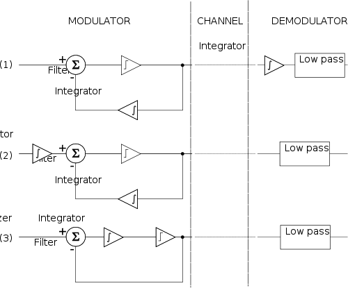 Fig. 2: Derivation of ΔΣ- from Δ-modulation
ΔΣ modulation (SDM) is inspired by Δ modulation (DM), as shown in Fig. 2. If quantization was homogeneous (e.g., if it was linear), the following would be a sufficient derivation of the equivalence of DM and SDM:
- Start with a block diagram of a Δ-modulator/demodulator.
- The linearity property of integration (
 ) makes it possible to move the integrator, which reconstructs the analog signal in the demodulator section, in front of the Δ-modulator.
 - Again, the linearity property of the integration allows the two integrators to be combined and a ΔΣ-modulator/demodulator block diagram is obtained.
However, the quantizer is not homogeneous, and so this explanation is flawed. It's true that ΔΣ is inspired by Δ-modulation, but the two are distinct in operation. From the first block diagram in Fig. 2, the integrator in the feedback path can be removed if the feedback is taken directly from the input of the low-pass filter. Hence, for delta modulation of input signal
 , the low-pass filter sees the signal
However, sigma-delta modulation of the same input signal places at the low-pass filter
In other words, SDM and DM swap the position of the integrator and quantizer. The net effect is a simpler implementation that has the added benefit of shaping the quantization noise away from signals of interest (i.e., signals of interest are low-pass filtered while quantization noise is high-pass filtered). This effect becomes more dramatic with increased oversampling, which allows for quantization noise to be somewhat programmable. On the other hand, Δ-modulation shapes both noise and signal equally.
Additionally, the quantizer (e.g., comparator) used in DM has a small output representing a small step up and down the quantized approximation of the input while the quantizer used in SDM must take values outside of the range of the input signal, as shown in Fig. 3.
 Fig. 3: An example of SDM of 100 samples of one period a sine wave. 1-bit samples (e.g., comparator output) overlaid with sine wave where logic high (e.g.,
 ) represented by blue and logic low (e.g.,
  ) represented by white.
In general, ΔΣ has some advantages versus Δ modulation:
- The whole structure is simpler:
- Only one integrator is needed
- The demodulator can be a simple linear filter (e.g., RC or LC filter) to reconstruct the signal
- The quantizer (e.g., comparator) can have full-scale outputs
- The quantized value is the integral of the difference signal, which makes it less sensitive to the rate of change of the signal.
Principle
The principle of the ΔΣ architecture is to make rough evaluations of the signal, to measure the error, integrate it and then compensate for that error. The mean output value is then equal to the mean input value if the integral of the error is finite. A demonstration applet is available online to simulate the whole architecture.[2]
Variations
There are many kinds of ADC that use this delta-sigma structure. The above analysis focuses on the simplest 1st-order, 2-level, uniform-decimation sigma-delta ADC. Many ADCs use a second-order 5-level sinc3 sigma-delta structure.
2nd order and higher order modulator
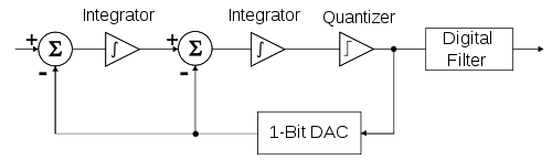 Fig. 4: Block diagram of a 2nd order ΔΣ modulator
The number of integrators, and consequently, the numbers of feedback loops, indicates the order of a ΔΣ-modulator; a 2nd order ΔΣ modulator is shown in Fig. 4. First order modulators are unconditionally stable, but stability analysis must be performed for higher order modulators.
3-level and higher quantizer
The modulator can also be classified by the number of bits it has in output, which strictly depends on the output of the quantizer. The quantizer can be realized with a N-level comparator, thus the modulator has log2N-bit output. A simple comparator has 2 levels and so is 1 bit quantizer; a 3-level quantizer is called a "1.5" bit quantizer; a 4-level quantizer is a 2 bit quantizer; a 5-level quantizer is called a "2.5 bit" quantizer.[3]
Decimation structures
The conceptually simplest decimation structure is a counter that is reset to zero at the beginning of each integration period, then read out at the end of the integration period.
The multi-stage noise shaping (MASH) structure has a noise shaping property, and is commonly used in digital audio and fractional-N frequency synthesizers. It comprises two or more cascaded overflowing accumulators, each of which is equivalent to a first-order sigma delta modulator. The carry outputs are combined through summations and delays to produce a binary output, the width of which depends on the number of stages (order) of the MASH. Besides its noise shaping function, it has two more attractive properties:
- simple to implement in hardware; only common digital blocks such as accumulators, adders, and D flip-flops are required
- unconditionally stable (there are no feedback loops outside the accumulators)
A very popular decimation structure is the sinc filter. For 2nd order modulators, the sinc3 filter is close to optimum.[4][5]
Quantization theory formulas
Main article: QuantizationWhen a signal is quantized, the resulting signal approximately has the second-order statistics of a signal with independent additive white noise. Assuming that the signal value is in the range of one step of the quantized value with an equal distribution, the root mean square value of this quantization noise is
In reality, the quantization noise is of course not independent of the signal; this dependence is the source of idle tones and pattern noise in Sigma-Delta converters.
Oversampling ratio, where fs is the sampling frequency and 2f0 is Nyquist rate
The rms noise voltage within the band of interest can be expressed in terms of OSR
Oversampling
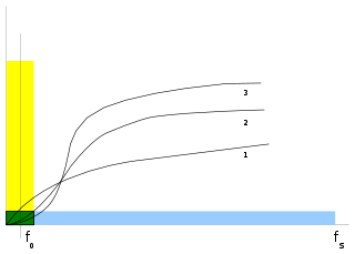 Fig. 5: Noise shaping curves and noise spectrum in ΔΣ modulatorMain article: Oversampling
Let's consider a signal at frequency
 and a sampling frequency of
  much higher than Nyquist rate (see fig. 5). ΔΣ modulation is based on the technique of oversampling to reduce the noise in the band of interest (green), which also avoids the use of high-precision analog circuits for the anti-aliasing filter. The quantization noise is the same both in a Nyquist converter (in yellow) and in an oversampling converter (in blue), but it is distributed over a larger spectrum. In ΔΣ-converters, noise is further reduced at low frequencies, which is the band where the signal of interest is, and it is increased at the higher frequencies, where it can be filtered. This technique is known as noise shaping.
For a first order delta sigma modulator, the noise is shaped by a filter with transfer function
![\scriptstyle H_n(z) \,=\, \left[1 - z^{-1}\right]](1/a6135265676869e701d5acdb0101f2b1.png) . Assuming that the sampling frequency
. Assuming that the sampling frequency  , the quantization noise in the desired signal bandwidth can be approximated as:
 .
.Similarly for a second order delta sigma modulator, the noise is shaped by a filter with transfer function
![\scriptstyle H_n(z) \,=\, \left[1 - z^{-1}\right]^2](8/2481c49d584c311191d1f43277ff620c.png) . The in-band quantization noise can be approximated as:
. The in-band quantization noise can be approximated as: .
.In general, for a
 -order ΔΣ-modulator, the variance of the in-band quantization noise:
 .
.When the sampling frequency is doubled, the signal to quantization noise is improved by
 for a -order ΔΣ-modulator. The higher the oversampling ratio, the higher the signal-to-noise ratio and the higher the resolution in bits.
Another key aspect given by oversampling is the speed/resolution tradeoff. In fact, the decimation filter put after the modulator not only filters the whole sampled signal in the band of interest (cutting the noise at higher frequencies), but also reduces the frequency of the signal increasing its resolution. This is obtained by a sort of averaging of the higher data rate bitstream.
Example of decimation
Let's have, for instance, an 8:1 decimation filter and a 1-bit bitstream; if we have an input stream like 10010110, counting the number of ones, the decimation result is 4/8 = 0.5 = 100b (binary); in other words,
- the sample frequency is reduced by a factor of eight
- the serial (1-bit) input bus becomes a parallel (3-bits) output bus.
Naming
The technique was first presented in the early 1960s by prof. Haruhiko Yasuda while he was student at Waseda University, Tokyo, Japan,[citation needed] The name Delta-Sigma comes directly from the presence of a Delta modulator and an integrator, as firstly introduced by Inose et al. in their patent application.[6] That is, the name comes from integrating or "summing" differences, which are operations usually associated with Greek letters Sigma and Delta respectively. Both names Sigma-Delta and Delta-Sigma are frequently used.
See also
References
- ^ Voltage-to-Frequency Converters by Walt Kester and James Bryant 2009. Analog Devices.
- ^ Analog Devices : Virtual Design Center : Interactive Design Tools : Sigma-Delta ADC Tutorial
- ^ Sigma-delta class-D amplifier and control method for a sigma-delta class-D amplifier by Jwin-Yen Guo and Teng-Hung Chang
- ^ A Novel Architecture for DAQ in Multi-channel, Large Volume, Long Drift Liquid Argon TPC by S. Centro, G. Meng, F. Pietropaola, S. Ventura 2006
- ^ A Low Power Sinc3 Filter for ΣΔ Modulators by A. Lombardi, E. Bonizzoni, P. Malcovati, F. Maloberti 2007
- ^ H. Inose, Y. Yasuda, J. Murakami, "A Telemetering System by Code Manipulation -- ΔΣ Modulation", IRE Trans on Space Electronics and Telemetry, Sep. 1962, pp. 204-209.
- Walt Kester (2008-10). "ADC Architectures III: Sigma-Delta ADC Basics" (PDF). Analog Devices. http://www.analog.com/static/imported-files/tutorials/MT-022.pdf. Retrieved 2010-11-02.
- R. Jacob Baker (2009). CMOS Mixed-Signal Circuit Design (2nd ed.). Wiley-IEEE. ISBN 978-0-470-29026-2. http://CMOSedu.com/.
- R. Schreier, G. Temes (2005). Understanding Delta-Sigma Data Converters. ISBN 0-471-46585-2.
- S. Norsworthy, R. Schreier, G. Temes (1997). Delta-Sigma Data Converters. ISBN 0-7803-1045-4.
- J. Candy, G. Temes (1992). Oversampling Delta-sigma Data Converters. ISBN 0-87942-285-8.
External links
- 1-bit A/D and D/A Converters
- Sigma-delta techniques extend DAC resolution article by Tim Wescott 2004-06-23
- Tutorial on Designing Delta-Sigma Modulators: Part I and Part II by Mingliang (Michael) Liu
- Gabor Temes' Publications
- Simple Sigma Delta Modulator example Contains Block-diagrams, code, and simple explanations
- Example Simulink model & scripts for continuous-time sigma-delta ADC Contains example matlab code and Simulink model
- Bruce Wooley's Delta-Sigma Converter Projects
- An Introduction to Delta Sigma Converters (which covers both ADC's and DAC's sigma-delta)
- Demystifying Sigma-Delta ADCs. This in-depth article covers the theory behind a Delta-Sigma analog-to-digital converter.
- Motorola digital signal processors: Principles of sigma-delta modulation for analog-to-digital converters
- One-Bit Delta Sigma D/A Conversion Part I: Theory article by Randy Yates presented at the 2004 comp.dsp conference
- MASH (Multi-stAge noise SHaping) structure with both theory and a block-level implementation of a MASH
- How a Sigma-Delta ADC Works at TechOnline free registration required to read the article
- Continuous time sigma-delta ADC noise shaping filter circuit architectures discusses architectural trade-offs for continuous-time sigma-delta noise-shaping filters
- Some intuitive motivation for why a Delta Sigma modulator works
Categories:


Wikimedia Foundation. 2010.