- Nano-RAM
-
Computer memory types Volatile - RAM
- In development
- Historical
Non-volatile - ROM
- Flash memory
- Early stage
- In development
- Historical
Nano-RAM is a proprietary computer memory technology from the company Nantero. It is a type of nonvolatile random access memory based on the mechanical position of carbon nanotubes deposited on a chip-like substrate. In theory, the small size of the nanotubes allows for very high density memories. Nantero also refers to it as NRAM.
Contents
Technology
The first generation Nantero NRAM technology was based on a three-terminal semiconductor device where a third terminal is used to switch the memory cell between memory states. The second generation NRAM technology is based on a two-terminal memory cell. The two-terminal cell has advantages such as a smaller cell size, better scalability to sub-20 nm nodes (see semiconductor device fabrication), and the ability to passivate the memory cell during fabrication.
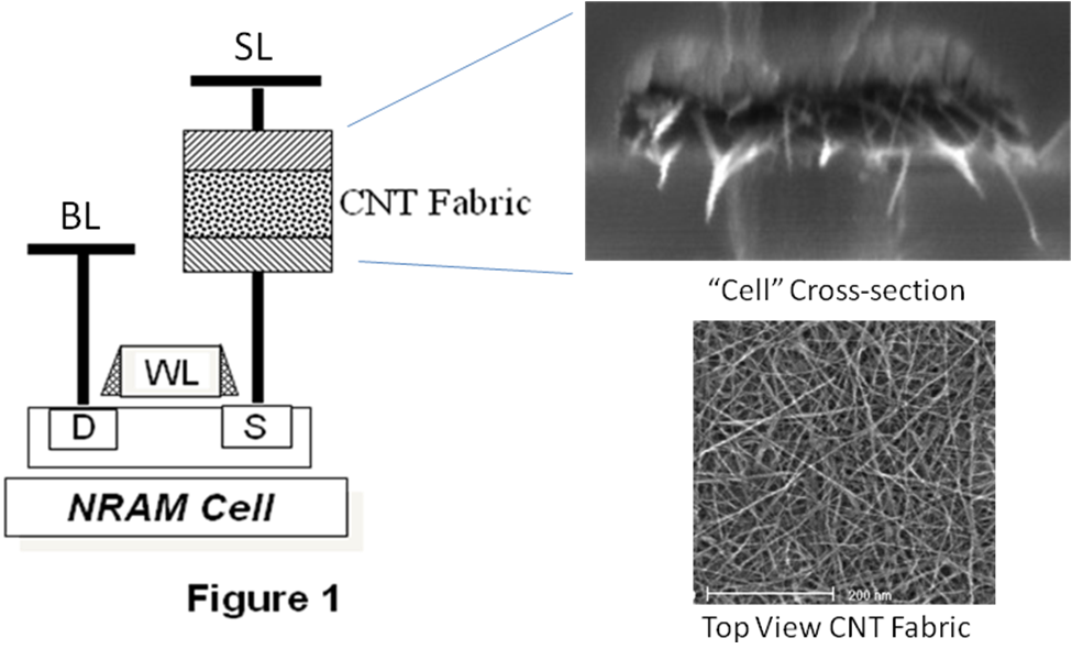
Nantero's technology is based on a well-known effect that in a non-woven fabric matrix of carbon nanotubes (CNTs), crossed nanotubes can either be touching or slightly separated depending on their mechanical state. When close to each other, the carbon nanotubes come under the influence of Van der Waal's forces. Each NRAM "cell" consists of an interlinked network of CNTs located between two electrodes as illustrated in Fig. 1. The CNT fabric is located between two metal electrodes, which is defined and etched by photolithography, and forms the NRAM cell.
 Carbon Nanotube Fabric
The NRAM acts as a resistive non-volatile random access memory (RAM) and can be placed in two or more resistive modes depending on the resistive state of the CNT fabric. When the CNTs are not in contact the resistance state of the fabric is high and represents a 0 (zero) state. When the CNTs are brought into contact, the resistance state of the fabric is low and represents a 1 state. NRAM can act as a memory because the two resistive states of the CNTs are both very stable. In the OFF or 0 state, the CNTs (or a portion of them) are not in contact and remain in a separated state due to the stiffness of the CNTs resulting in a high resistance or low current measurement state between the top and bottom electrodes. In the ON or 1 state, the CNTs (or a portion of them) are in contact and remain in a contacted state due to Van der Waals forces between the CNTs resulting in a low resistance or high current measurement state between the top and bottom electrodes.
To switch the NRAM between states, a small voltage greater than the read voltage is applied between top and bottom electrodes. If the NRAM is in the 0 state, the voltage applied will cause an electrostatic attraction between the CNTs close each other causing a SET operation. After the applied voltage is removed, the CNTs remain in an ON or low resistance state due to physical adhesion (Van der Waals force) with an activation energy (Ea) of approximately 5eV. If the NRAM cell is in the 1 state, applying a voltage greater than the read voltage will generate CNT phonon excitations with sufficient energy to separate the CNT junctions. This is the phonon driven RESET operation. The CNTs remain in the OFF or high resistance state due to the high mechanical stiffness (Young's Modulus 1 TPa) with an activation energy (Ea) much greater than 5 eV. Figure 2 illustrates both states of an individual pair of CNTs involved in the switch operation. Due to the high activation energy (> 5eV) required for switching between states, the NRAM switch shows excellent resistance to outside interference like radiation and operating temperature that can erase or flip conventional memories like DRAM.
 Fig. 2: Carbon Nanotube Contact Points
NRAMs are fabricated by depositing a uniform layer of CNTs onto a prefabricated array of drivers such as transistors as shown in Figure 1. The bottom electrode of the NRAM cell is in contact with the underlying via (electronics) connecting the cell to the driver. The bottom electrode may be fabricated as part of the underlying via or it may be fabricated simultaneously with the NRAM cell, when the cell is photolithographically defined and etched. Before the cell is photolithographically defined and etched, the top electrode is deposited as a metal film onto the CNT layer so that the top metal electrode is patterned and etched during the definition of the NRAM cell. Following the dielectric passivation and fill of the array, the top metal electrode is exposed by etching back the overlying dielectric using a smoothing process such as CMP (Chemical-mechanical planarization). With the top electrode exposed, the next level of metal wiring interconnect is fabricated to complete the NRAM array. Figure 3 illustrates one of the many circuit methods that can be used to select a single cell for writing and reading. Using a cross-grid interconnect arrangement, the NRAM and driver, (the cell), forms a memory array similar to other memory arrays such as DRAM or Flash memory. A single cell can be selected by applying the proper voltages to the word line (WL), bit line (BL), and select lines (SL) without disturbing the other cells in the array.
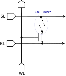 Fig. 3: CNT Switch
Advantages
NRAM has a density, at least in theory, similar to that of DRAM. DRAM consists of a number of capacitors, which are essentially two small metal plates with a thin insulator between them. NRAM is similar, with the terminals and electrodes being roughly the same size as the plates in a DRAM, the nanotubes between them being so much smaller they add nothing to the overall size. However it seems there is a minimum size at which a DRAM can be built, below which there simply not enough charge is being stored on the plates to be effectively read. NRAM appears to be limited only by the current state of the art in lithography. This means that NRAM may be able to become much denser than DRAM, meaning that it will also be less expensive. Additionally, unlike DRAM, NRAM does not require power to "refresh" it, and will retain its memory even after power is removed. Thus the power needed to write and retain the memory state of the device is much lower than DRAM, which has to build up charge on the cell plates. This means that NRAM will not only compete with DRAM in terms of cost, but will require much less power to run, and as a result also be much faster because write performance is largely determined by the total charge needed. NRAM can theoretically reach performance similar to SRAM, which is faster than DRAM but much less dense, and thus much more expensive.
Compared other NVRAM ("Non-Volatile RAM") technologies, NRAM has further advantages. The most common form of NVRAM today is FLASH RAM. In Flash Memory, each cell resembles a MOSFET transistor with a control gate (CG) modulated by a floating gate (FG) interposed between the CG and the FG. The FG is surrounded by an insulating dielectric, typically an oxide. Since the FG is electrically isolated by the surrounding dielectric, any electrons placed on the FG will be trapped on the FG which screens the CG from the channel of the transistor and modifies the threshold voltage (VT) of the transistor. By writing and controlling the amount of charge placed on the FG, the FG controls the conduction state of the MOSFET FLASH device depending on the VT of the cell selected. The current flowing through the MOSFET channel is sensed to determine the state of the cell forming a binary code where a 1 state (current flow) when an appropriate CG voltage is applied and a 0 state (no current flow) when the CG voltage is applied.
After being written to, the insulator traps electrons on the FG, locking it into the 0 state. However, in order to change that bit the insulator has to be "overcharged" to erase any charge already stored in it. This requires higher voltage, about 10 volts, much more than a battery can provide. FLASH systems include a "charge pump" that slowly builds up power and releases it at higher voltage. This process is not only very slow, but degrades the insulators as well. For this reason FLASH has a limited lifetime, between 10,000 and 1,000,000 "writes" before the device will no longer operate effectively.
NRAM potentially avoids all of these issues. The read and write process are both "low energy" in comparison to Flash (or DRAM for that matter due to "refresh"), meaning that NRAM can result in longer battery life in conventional devices. It may also be much faster to write than either, meaning it may be used to replace both. A modern cell phone will often include FLASH memory for storing phone numbers and such, DRAM for higher performance working memory because FLASH is too slow, and additionally some SRAM in the CPU because DRAM is too slow for its own use. With NRAM all of these may be replaced, with some NRAM placed on the CPU to act as the CPU cache, and more in other chips replacing both the DRAM and FLASH.
Comparison with other proposed systems
NRAM is one of a variety of new memory systems, many of which claim to be "universal" in the same fashion as NRAM – replacing everything from Flash to DRAM to SRAM.
The only alternative memory currently ready for commercial use is ferroelectric RAM (FRAM or FeRAM). FeRAM adds a small amount of a ferro-electric material in an otherwise "normal" DRAM cell, the state of the field in the material encoding the bit in a non-destructive format. FeRAM has all of the advantages of NRAM, although the smallest possible cell size is much larger than for NRAM. FeRAM is currently in use in a number of applications where the limited number of writes in Flash is an issue. The FeRAM read operation is inherently destructive, requiring a restoring write operation afterwards.
Other more speculative memory systems include MRAM and PRAM. MRAM is based on a grid of magnetic tunnel junctions. Key to MRAM's potential is the way it reads the memory using the tunnel magnetoresistive effect, allowing it to read the memory both non-destructively and with very little power. Unfortunately, the 1st generation MRAM, which utilized field induced writing,[1] reached a limit in terms of size, which kept it much larger than existing Flash devices. However, two new MRAM techniques are currently in development and hold the promises of overcoming the size limitaion and making MRAM more competitive even with Flash memory. The techniques are Thermal Assisted Switching (TAS),[2] which is being developed by Crocus Technology, and Spin Torque Transfer (STT) on which Crocus, Hynix, IBM, and several other companies are working.[3]
PRAM is based on a technology similar to that in a writable CD or DVD, using a phase-change material that changes its magnetic or electrical properties instead of its optical ones. The PRAM material itself is scalable but requires a larger current source.
Due to the massive investment in FLASH factories (Semiconductor fabrication plant), no alternative memory has yet been able to replace FLASH in the marketplace.
See also
References
- ^ http://www.everspin.com/technology.php
- ^ The Emergence of Practical MRAM http://www.crocus-technology.com/pdf/BH%20GSA%20Article.pdf
- ^ http://www.eetimes.com/news/latest/showArticle.jhtml?articleID=218000269
External links
- Nantero's NRAM page
- On the tube - A new type of computer memory uses carbon, rather than silicon (Economist magazine)


Wikimedia Foundation. 2010.