- Wafer (electronics)
-
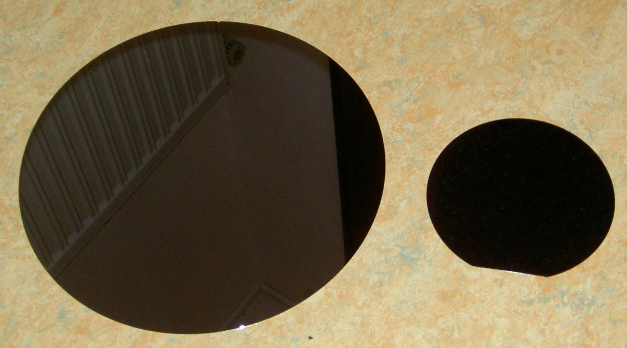
 Polished 12" and 6" silicon wafers. The flat cut into the right wafer indicates its doping and crystallographic orientation (see below)
A wafer is a thin slice of semiconductor material, such as a silicon crystal, used in the fabrication of integrated circuits and other microdevices. The wafer serves as the substrate for microelectronic devices built in and over the wafer and undergoes many microfabrication process steps such as doping or ion implantation, etching, deposition of various materials, and photolithographic patterning. Finally the individual microcircuits are separated (dicing) and packaged.
Several types of solar cell are also made from such wafers. On a solar wafer a solar cell (usually square) is made from the entire wafer.
Contents
Formation
See also: Ingot The Czochralski process.
 2-inch (51 mm), 4-inch (100 mm), 6-inch (150 mm), and 8-inch (200 mm) wafers
Wafers are formed of highly pure (99.9999% purity),[1] nearly defect-free single crystalline material.[2] One process for forming crystalline wafers is known as Czochralski growth invented by the Polish chemist Jan Czochralski. In this process, a cylindrical ingot of high purity monocrystalline silicon is formed by pulling a seed crystal from a 'melt'.[3][4] Dopant impurity atoms such as boron or phosphorus can be added to the molten intrinsic silicon in precise amounts in order to dope the silicon, thus changing it into n-type or p-type extrinsic silicon.
The ingot is then sliced with a wafer saw (wire saw) and polished to form wafers.[5] The size of wafers for photovoltaics is 100–200 mm square and the thickness is 200–300 μm. In the future, 160 μm will be the standard.[6] Electronics use wafer sizes from 100–300 mm diameter. (The largest wafer made has a diameter of 450 mm but is not in production yet.)
Cleaning, texturing and etching
Wafers are cleaned with weak acids to remove unwanted particles, or repair damage caused during the sawing process. When used for solar cells, the wafers are textured to create a rough surface to increase their efficiency. The generated PSG (phosphosilicate glass) is removed from the edge of the wafer in the etching.[7]
Wafer properties
Standard wafer sizes
Silicon wafers are available in a variety of sizes from 25.4 mm (1 inch) to 300 mm (11.8 inches).[8] Semiconductor fabrication plants (also known as fabs) are defined by the size of wafers that they are tooled to produce. The size has gradually increased to improve throughput and reduce cost with the current state-of-the-art fab considered to be 300 mm (12 inch), with the next standard projected to be 450 mm (18 inch).[9][10] Intel, TSMC and Samsung are separately conducting research to the advent of 450 mm "prototype" (research) fabs by 2012, though serious hurdles remain. Dean Freeman, an analyst with Gartner Inc., predicted that production fabs could emerge sometime between the 2017 and 2019 timeframe,[11] a lot of that will depend on a plethora of new technological breakthroughs and not simply extending current technology.
- 1-inch (25 mm)
- 2-inch (51 mm). Thickness 275 µm.
- 3-inch (76 mm). Thickness 375 µm.
- 4-inch (100 mm). Thickness 525 µm.
- 5-inch (130 mm) or 125 mm (4.9 inch). Thickness 625 µm.
- 150 mm (5.9 inch, usually referred to as "6 inch"). Thickness 675 µm.
- 200 mm (7.9 inch, usually referred to as "8 inch"). Thickness 725 µm.
- 300 mm (11.8 inch, usually referred to as "12 inch"). Thickness 775 µm.
- 450 mm ("18 inch"). Thickness 925 µm (expected).[12]
Wafers grown using materials other than silicon will have different thicknesses than a silicon wafer of the same diameter. Wafer thickness is determined by the mechanical strength of the material used; the wafer must be thick enough to support its own weight without cracking during handling.
A unit wafer fabrication step, such as an etch step or a lithography step, can be performed on more chips per wafer as roughly the square of the increase in wafer diameter, while the cost of the unit fabrication step goes up more slowly than the square of the wafer diameter. This is the cost basis for shifting to larger and larger wafer sizes. Conversion to 300 mm wafers from 200 mm wafers began in earnest in 2000, and reduced the price per die about 30-40%.[13] However, this was not without significant problems for the industry.
The next step to 450 mm should accomplish similar productivity gains as the previous size increase. However, machinery needed to handle and process larger wafers results in increased investment costs to build a single factory. There is considerable resistance to moving up to 450 mm by 2012 despite the obvious productivity enhancements, mainly because companies feel it would take too long to recoup their investment.[14] The difficult and costly 300 mm process only accounted for approximately 20% of worldwide capacity on a square inches basis by the end of 2005.[15] The step up to 300 mm required a major change from the past, with fully automated factories using 300 mm wafers versus barely automated factories for the 200 mm wafers. These major investments were undertaken in the economic downturn following the dot-com bubble, resulting in huge resistance to upgrading to 450 mm by the original timeframe.
Other initial technical problems in the ramp up to 300 mm included vibrational effects, gravitational bending (sag), and problems with flatness. Among the new problems in the ramp up to 450 mm are that the crystal ingots will be 3 times heavier (total weight a metric ton) and take 2-4 times longer to cool, and the process time will be double.[16] All told, the development of 450 mm wafers require significant engineering, time, and cost to overcome.
Analytical die count estimation
For any given wafer diameter [d, mm] and target IC size [S, mm2], there is an exact number of integral die pieces that can be sliced out of the wafer. The gross Die Per Wafer [DPW] can be estimated by the following expression:

Note, that the gross die count does not take into account the die defect loss, various alignment markings and test sites on the wafer.
Crystalline orientation
 Diamond Cubic Crystal Structure, Silicon unit cell
 Flats can be used to denote doping and crystallographic orientation. Red represents material that has been removed.
Wafers are grown from crystal having a regular crystal structure, with silicon having a diamond cubic structure with a lattice spacing of 5.430710 Å (0.5430710 nm).[17] When cut into wafers, the surface is aligned in one of several relative directions known as crystal orientations. Orientation is defined by the Miller index with [100] or [111] faces being the most common for silicon.[17] Orientation is important since many of a single crystal's structural and electronic properties are highly anisotropic. Ion implantation depths depend on the wafer's crystal orientation, since each direction offers distinct paths for transport.[18] Wafer cleavage typically occurs only in a few well-defined directions. Scoring the wafer along cleavage planes allows it to be easily diced into individual chips ("dies") so that the billions of individual circuit elements on an average wafer can be separated into many individual circuits.
Wafer flats and crystallographic orientation notches
Wafers under 200 mm diameter have flats cut into one or more sides indicating the crystallographic planes of the wafer (usually the {110} face). In earlier-generation wafers a pair of flats at different angles additionally conveyed the doping type (see illustration for conventions). Wafers of 200 mm diameter and above use a single small notch to convey wafer orientation, with no visual indication of doping type.[19]
Impurity doping
Silicon wafers are generally not 100% pure silicon, but are instead formed with an initial impurity doping concentration between 1013 and 1016 per cm3 of boron, phosphorus, arsenic, or antimony which is added to the melt and defines the wafer as either bulk n-type or p-type.[20] However, compared with single-crystal silicon's atomic density of 5×10²² atoms per cm3, this still gives a purity greater than 99.9999%. The wafers can also be initially provided with some interstitial oxygen concentration. Carbon and metallic contamination are kept to a minimum.[21] Transition metals, in particular, must be kept below parts per billion concentrations for electronic applications.[22]
Compound semiconductors
While silicon is the prevalent material for wafers used in the electronics industry, other compound III-V or II-VI materials have also been employed. Gallium arsenide (GaAs), a III-V semiconductor produced via the Czochralski process, is also a common wafer material.[4]
See also
- Monocrystalline silicon
- Epilayer
- Epitaxy
- Junction
- Layer (electronics)
- Low-cost solar cell
- Rapid thermal processing
- Refining
- Screen printing
- SEMI font
- Silicon on insulator (SOI) wafers
- Solar panel
- RCA clean
- Melting
- Klaiber's law
- Wafer bonding
References
- ^ "Semi" SemiSource 2006: A supplement to Semiconductor International. December 2005. Reference Section: How to Make a Chip. Adapted from Design News. Reed Electronics Group.
- ^ SemiSource 2006: A supplement to Semiconductor International. December 2005. Reference Section: How to Make a Chip. Adapted from Design News. Reed Electronics Group.
- ^ Levy, Roland Albert (1989). Microelectronic Materials and Processes. pp. 1–2. ISBN 0792301544. http://books.google.com/books?id=wZPRPU6ne7UC&pg=PA248#PPA6,M1. Retrieved 2008-02-23.
- ^ a b Grovenor, C. (1989). Microelectronic Materials. CRC Press. pp. 113–123. ISBN 0852742703. http://books.google.com/books?id=Ecl_mnz1xcUC&pg=PA122&dq=GaAs+Wafer+Manufacture#PPA113,M1. Retrieved 2008-02-25.
- ^ Nishi, Yoshio (2000). Handbook of Semiconductor Manufacturing Technology. CRC Press. pp. 67–71. ISBN 0824787838. http://books.google.com/books?id=Qi98H-iTgLEC&pg=PA70&dq=wafer+flat+and+notch#PPA71,M1. Retrieved 2008-02-25.
- ^ http://www.omron-semi-pv.eu/en/wafer-based-pv/wafer-preparation/slicing-the-ingot.html
- ^ http://www.omron-semi-pv.eu/en/wafer-based-pv/front-end/wet-process.html
- ^ "Silicon Wafer". http://www.semiwafer.com/products/silicon.htm. Retrieved 2008-02-23.
- ^ Intel, Samsung, TSMC reach agreement about 450mm tech
- ^ Presentations/PDF/FEP.pdf ITRS Presentation (PDF)
- ^ Industry Agrees on first 450-mm wafer standard - EETimes.com, retrieved on October 22, 2008.
- ^ Industry Agrees on first 450-mm wafer standard - EETimes.com
- ^ Semiconductor.net:Capability for 300 mm: Approaching Industry Goals
- ^ 450 mm: A Promise Postponed
- ^ A Simulation Study of the Cost and Economics of 450 mm Wafers
- ^ Semiconducter.net:Optimize Wafer Thickness for 450 mm
- ^ a b O'Mara, William C. (1990). Handbook of Semiconductor Silicon Technology. William Andrew Inc.. pp. 349–352. ISBN 0815512376. http://books.google.com/books?id=COcVgAtqeKkC&pg=PA351&dq=Czochralski+Silicon+Crystal+Face+Cubic. Retrieved 2008-02-24.
- ^ Nishi, Yoshio (2000). Handbook of Semiconductor Manufacturing Technology. CRC Press. pp. 108–109. ISBN 0824787838. http://books.google.com/books?id=Qi98H-iTgLEC&pg=PA70&dq=wafer+flat+and+notch#PPA71,M1. Retrieved 2008-02-25.
- ^ "Wafer Flats". http://www.tf.uni-kiel.de/matwis/amat/elmat_en/kap_5/illustr/i5_2_4.html. Retrieved 2008-02-23.
- ^ Widmann, Dietrich (2000). Technology of Integrated Circuits. Springer. pp. 39. ISBN 3540661999. http://books.google.com/books?id=uYNn1N6YSwQC&pg=PA39&dq=Czochralski+Doping+Silicon. Retrieved 2008-02-24.
- ^ Levy, Roland Albert (1989). Microelectronic Materials and Processes. pp. 6–7, 13. ISBN 0792301544. http://books.google.com/books?id=wZPRPU6ne7UC&pg=PA248#PPA1,M1. Retrieved 2008-02-23.
- ^ Rockett, Angus (2008). The Materials Science of Semiconductors. pp. 13. ISBN 9780387256535.
12
External links
- Everything Wafers - A guide to semiconductor substrates type, property, cleaving, etching, and fabrication.
Categories:


Wikimedia Foundation. 2010.