- Distributed element model
-
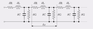 Fig.1 Transmission line. The distributed element model applied to a transmission line.
- This article is an example from the domain of electrical systems, which is a special case of the more general distributed parameter systems.
In electrical engineering, the distributed element model or transmission line model of electrical circuits assumes that the attributes of the circuit (resistance, capacitance, and inductance) are distributed continuously throughout the material of the circuit. This is in contrast to the more common lumped element model, which assumes that these values are lumped into electrical components that are joined by perfectly conducting wires. In the distributed element model, each circuit element is infinitesimally small, and the wires connecting elements are not assumed to be perfect conductors; that is, they have impedance. Unlike the lumped element model, it assumes non-uniform current along each branch and non-uniform voltage along each node. The distributed model is used at high frequencies where the wavelength approaches the physical dimensions of the circuit, making the lumped model inaccurate.
Contents
Applications
The distributed element model is more accurate but more complex than the lumped element model. The use of infinitesimals will often require the application of calculus whereas circuits analysed by the lumped element model can be solved with linear algebra. The distributed model is consequently only usually applied when accuracy calls for its use. Where this point is depends on the accuracy required in a specific application, but essentially, it needs to be used in circuits where the wavelengths of the signals have become comparable to the physical dimensions of the components. An often quoted engineering rule of thumb (not to be taken too literally because there are many exceptions) is that parts larger than one tenth of a wavelength will usually need to be analysed as distributed elements.[1]
Transmission lines
Transmission lines are a common example of the use of the distributed model. Its use is dictated because the length of the line will usually be many wavelengths of the circuit's operating frequency. Even for the low frequencies used on power transmission lines, one tenth of a wavelength is still only about 500 kilometres at 60 Hz. Transmission lines are usually represented in terms of the primary line constants as shown in figure 1. From this model the behaviour of the circuit is described by the secondary line constants which can be calculated from the primary ones.
The primary line constants are normally taken to be constant with position along the line leading to a particularly simple analysis and model. However, this is not always the case, variations in physical dimensions along the line will cause variations in the primary constants, that is, they have now to be described as functions of distance. Most often, such a situation represents an unwanted deviation from the ideal, such as a manufacturing error, however, there are a number of components where such longitudinal variations are deliberately introduced as part of the function of the component. A well known example of this is the horn antenna.
Where reflections are present on the line, quite short lengths of line can exhibit effects that are simply not predicted by the lumped element model. A quarter wavelength line, for instance, will transform the terminating impedance into its dual. This can be a wildly different impedance.
High frequency transistors
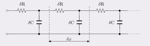 Fig.2. The base region of a bipolar junction transistor can be modelled as a simplified transmission line.
Another example of the use of distributed elements is in the modelling of the base region of a bipolar junction transistor at high frequencies. The analysis of charge carriers crossing the base region is not accurate when the base region is simply treated as a lumped element. A more successful model is a simplified transmission line model which includes distributed bulk resistance of the base material and distributed capacitance to the substrate. This model is represented in figure 2.
Resistivity measurements
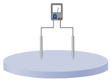 Fig. 3. Simplified arrangement for measuring resistivity of a bulk material with surface probes.
In many situations it is desired to measure resistivity of a bulk material by applying an electrode array at the surface. Amongst the fields that use this technique are geophysics (because it avoids having to dig into the substrate) and the semiconductor industry also use it (for the similar reason that it is non-intrusive) for testing bulk silicon wafers.[2] The basic arrangement is shown in figure 3, although normally more electrodes would be used. To form a relationship between the voltage and current measured on the one hand, and the resistivity of the material on the other, it is necessary to apply the distributed element model by considering the material to be an array of infinitesimal resistor elements. Unlike the transmission line example, the need to apply the distributed element model arises from the geometry of the setup, and not from any wave propagation considerations.[3]
The model used here needs to be truly 3-dimensional (transmission line models are usually described by elements of a one-dimensional line). It is also possible that the resistances of the elements will be functions of the co-ordinates, indeed, in the geophysical application it may well be that regions of changed resistivity are the very things that it is desired to detect.[4]
Inductor windings
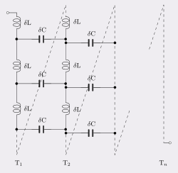 Fig. 4. A possible distributed element model of an inductor. A more accurate model will also require series resistance elements with the inductance elements.
Another example where a simple one-dimensional model will not suffice is the windings of an inductor. Coils of wire have capacitance between adjacent turns (and also more remote turns as well, but the effect progressively diminishes). For a single layer solenoid, the distributed capacitance will mostly lie between adjacent turns as shown in figure 4 between turns T1 and T2, but for multiple layer windings and more accurate models distributed capacitance to other turns must also be considered. This model is fairly difficult to deal with in simple calculations and for the most part is avoided. The most common approach is to roll up all the distributed capacitance into one lumped element in parallel with the inductance and resistance of the coil. This lumped model works successfully at low frequencies but falls apart at high frequencies where the usual practice is to simply measure (or specify) an overall Q for the inductor without associating a specific equivalent circuit.[5]
See also
- Distributed element filter
- Transmission line
- Lumped components
References
Bibliography
- Kenneth L. Kaiser, Electromagnetic compatibility handbook, CRC Press, 2004 ISBN 0849320879.
- Karl Lark-Horovitz, Vivian Annabelle Johnson, Methods of experimental physics: Solid state physics, Academic Press, 1959 ISBN 0124759467.
- Robert B. Northrop, Introduction to instrumentation and measurements, CRC Press, 1997 ISBN 0849378982.
- P. Vallabh Sharma, Environmental and engineering geophysics, Cambridge University Press, 1997 ISBN 0521576326.
Categories:- Electronic design
- Distributed element circuits


Wikimedia Foundation. 2010.