- Chemical beam epitaxy
-
Chemical beam epitaxy (CBE) forms an important class of deposition techniques for semiconductor layer systems, especially III-V semiconductor systems. This form of epitaxial growth is performed in an ultrahigh vacuum system. The reactants are in the form of molecular beams of reactive gases, typically as the hydride or a metalorganic. The term CBE is often used interchangeably with metal-organic molecular beam epitaxy (MOMBE). The nomenclature does differentiate between the two (slightly different) processes, however. When used in the strictest sense, CBE refers to the technique in which both components are obtained from gaseous sources, while MOMBE refers to the technique in which the group III component is obtained from a gaseous source and the group V component from a solid source.
Contents
Basic principles
Chemical Beam Epitaxy was first demonstrated by W.T. Tsang in 1984[1]. This technique was then described as a hybrid of metal-organic chemical vapor deposition (MOCVD) and molecular beam epitaxy (MBE) that exploited the advantages of both the techniques. In this initial work, InP and GaAs were grown using gaseous group III and V alkyls. While group III elements were derived from the pyrolysis of the alkyls on the surface, the group V elements were obtained from the decomposition of the alkyls by bringing in contact with heated Tantalum (Ta) or Molybdenum (Mo) at 950-1200 °C. Typical pressure in the gas reactor is between 102 Torr and 1 atm for MOCVD. Here, the transport of gas occurs by viscous flow and chemicals reach the surface by diffusion. In contrast, gas pressures of less than 10-4 Torr are used in CBE. The gas transport now occurs as molecular beam due to the much longer mean-free paths, and the process evolves to a chemical beam deposition.[2] It is also worth noting here that MBE employs atomic beams (such as aluminium (Al) and Gallium (Ga)) and molecular beams (such as As4 and P4) that are evaporated at high temperatures from solid elemental sources, while the sources for CBE are in vapor phase at room temperatures.[3] A comparison of the different processes in the growth chamber for MOCVD, MBE and CBE can be seen in figure 1.
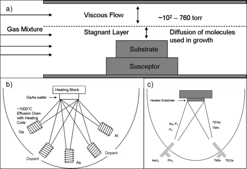 Figure 1: Basic processes inside the growth chambers of a) MOCVD, b) MBE, and c) CBE.[3]
Experimental Setup
A combination of turbomolecular and cryo pumps are used in standard UHV growth chambers. The chamber itself is equipped with a liquid nitrogen cryoshield and a rotatable crystal holder capable of carrying more than one wafer. The crystal holder is usually heated from the backside to temperatures of 500 to 700°C. Most setups also have RHEED equipment for the in-situ monitoring of surface superstructures on the growing surface and for measuring growth rates, and mass spectrometers for the analysis of the molecular species in the beams and the analysis of the residual gases.[4] The gas inlet system, which is one of the most important components of the system, controls the material beam flux. Pressure controlled systems are used most commonly. The material flux is controlled by the input pressure of the gas injection capillary. The pressure inside the chamber can be measured and controlled by a capacitance manometer. The molecular beams of gaseous source materials injectors or effusion jets that ensure a homogeneous beam profile. For some starting compounds, such as the hydrides that are the group V starting material, the hydrides have to be precracked into the injector. This is usually done by thermally decomposing with a heated metal or filament.[4]
Growth Kinetics
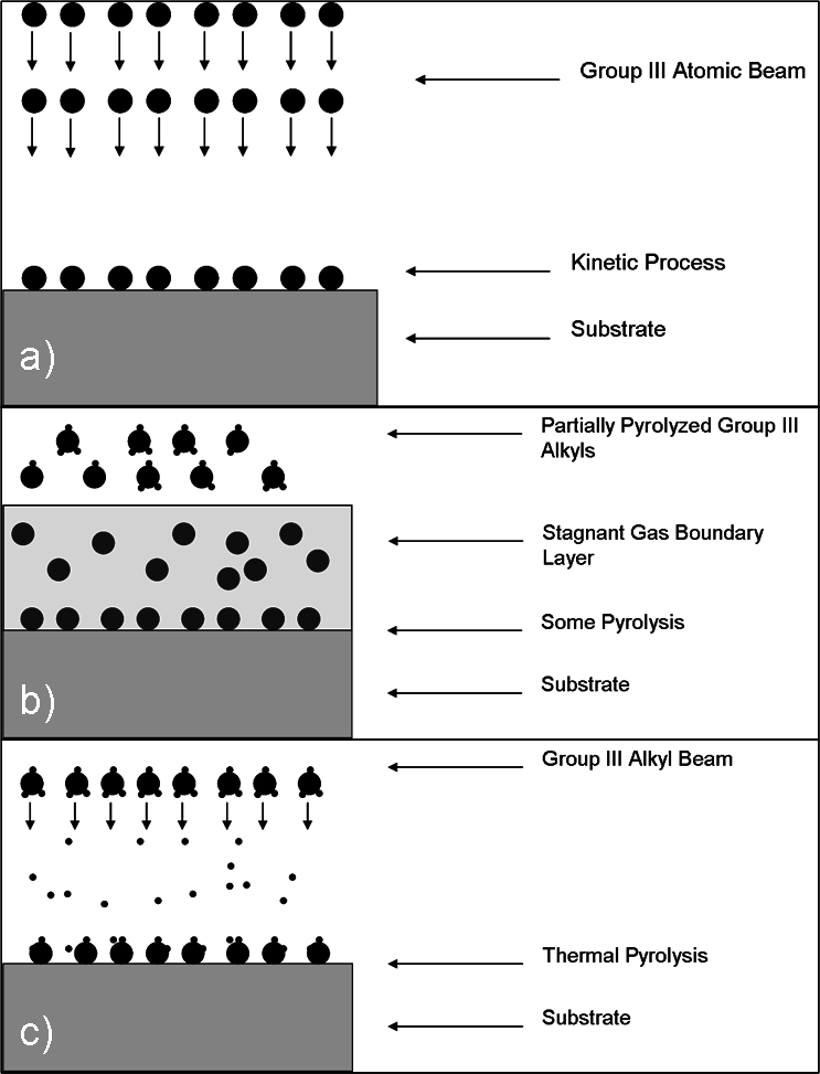
In order to better understand the growth kinetics associated with CBE, it is important to look at physical and chemical processes associated with MBE and MOCVD as well. Figure 2 depicts those. The growth kinetics for these three techniques differ in many ways. In conventional gas source MBE, the growth rate is determined by the arrival rate of the group III atomic beams. The epitaxial growth takes place as the group III atoms impinge on the heated substrate surface, migrates into the appropriate lattice sites and then deposits near excess group V dimers or tetramers. It is worth noting that no chemical reaction is involved at the surface since the atoms are generated by thermal evaporation from solid elemental sources.[2]
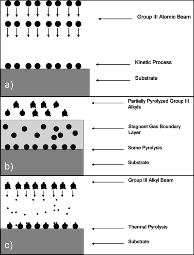 Figure 2: Growth kinetics involved in a) conventional MBE, b) MOCVD, and c) CBE. [2]
In MOCVD, group III alkyls are already partially dissociated in the gas stream. These diffuse through a stagnant boundary layer that exists over the heated substrate, after which they dissociate into the atomic group III elements. These atoms then migrate to the appropriate lattice site and deposit epitaxially by associating with a group V atom that was derived from the thermal decomposition of the hydrides. The growth rate here is usually limited by the diffusion rate of the group III alkyls through the boundary layer. Gas phase reactions between the reactants have also been observed in this process.[2]
In CBE processes, the hydrides are cracked in a high temperature injector before they reach the substrate. The temperatures are typically 100-150°C lower than they are in a similar MOCVD or MOVPE.[5] There is also no boundary layer (such as the one in MOCVD) and molecular collisions are minimal due to the low pressure. The group V alkyls are usually supplied in excess, and the group III alkyl molecules impinge directly onto the heated substrate as in conventional MBE. The group III alkyl molecule has two options when this happens. The first option is to dissociate its three alkyl radicals by acquiring thermal energy from the surface, and leaving behind the elemental group III atoms on the surface. The second option is to re-evaporate partially or completely undissociated. Thus, the growth rate is determined by the arrival rate of the group III alkyls at a higher substrate temperature, and by the surface pyrolysis rate at lower temperatures.[2]
Compatibility with Device Fabrication
Selective Growth at Low Temperatures
Selective growth through dielectric masking is readily achieved using CBE as compared to its parent techniques of MBE and MOCVD. Selective growth is hard to achieve using elemental source MBE because group III atoms do not desorb readily after they are adsorbed. With chemical sources, the reactions associated with the growth rate are faster on the semiconductor surface than on the dielectric layer. No group III element can, however, arrive at the dielectric surface in CBE due to the absence of any gas phase reactions. Also, it is easier for the impinging group III metalorganic molecules to desorb in the absence of the boundary layer. This makes it easier to perform selective epitaxy using CBE and at lower temperatures, compared to MOCVD or MOVPE.[5]
p-type Doping
It was observed that using TMGa for the CBE of GaAs led to high p-type background doping (1020 cm-3) due to incorporated carbon. However, it was found that using TEGa instead of TMGa led to very clean GaAs with room temperature hole concentrations between 1014 and 1016 cm-3. It has been demonstrated that the hole concentrations can be adjusted between 1014 and 1021 cm-3 by just adjusting the alkyl beam pressure and the TMGa/TEGa ratio, providing means for achieving high and controllable p-type doping of GaAs. This has been exploited for fabricating high quality heterojunction bipolar transistors.[4]
Advantages and Disadvantages of CBE
CBE offers many other advantages over its parent techniques of MOCVD and MBE, some of which are listed below:
Advantages over MBE
- Easier multiwafer scaleup: Substrate rotation is required for uniformity in thickness and conformity since MBE has individual effusion cells for each element. Large effusion cells and efficient heat dissipation make multiwafer scaleup more difficult.
- Better for production environment: Instant flux response due to precision electronic control flow.
- Absence of oval defects: These oval defects generally arise from micro-droplets of Ga or In spit out from high temperature effusion cells. These defects vary in size and density system-to-system and time-to-time.[3][6]
Advantages over MOCVD
- Easy implementation of in-situ diagnostic instruments such as RHEED.
- Compatibility with other high vacuum thin-film processing methods, such as metal evaporation and ion implantation.[3][6]
Shortcomings of CBE
- More pumping required compared to MOCVD.
- Composition control can be difficult when growing GaInAs. Incorporation of In from TMIn is significantly larger than that for Ga from TEGa at temperatures around 600°C.
- High carbon incorporation for GaAlAs.[3][6]
References
- ^ W.T. Tsang, “Chemical beam epitaxy of InP and GaAs”. Appl. Phys. Lett. 45, 1234 (1984).
- ^ a b c d e W.T. Tsang, “CBE of Ga0.47In0.53As/InP quantum wells and heterostructure devices”. J. Cryst. Growth. 81, 261 (1987).
- ^ a b c d e W.T. Tsang, “From Chemical Vapor Epitaxy to Chemical Beam Epitaxy”. J. Cryst. Growth. 95, 121 (1989).
- ^ a b c Hans Lűth, “Chemical beam epitaxy – a child of surface science”. Surface Science. 299, 867 (1994).
- ^ a b J. L. Benchimol, F. Alexandre, B. Lamare and P. Legay “Benefits of Chemical Beam Epitaxy for Micro and Optoelectronic Applications”. Prog. Crystal Growth and Charact. 33, 473 (1996).
- ^ a b c M.A. Herman and H. Sitter. Molecular Beam Epitaxy. Heidelberg: Springer, 1996.
See also
Categories:- Thin film deposition
- Semiconductor growth

Wikimedia Foundation. 2010.