- Voltage multiplier
-
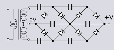
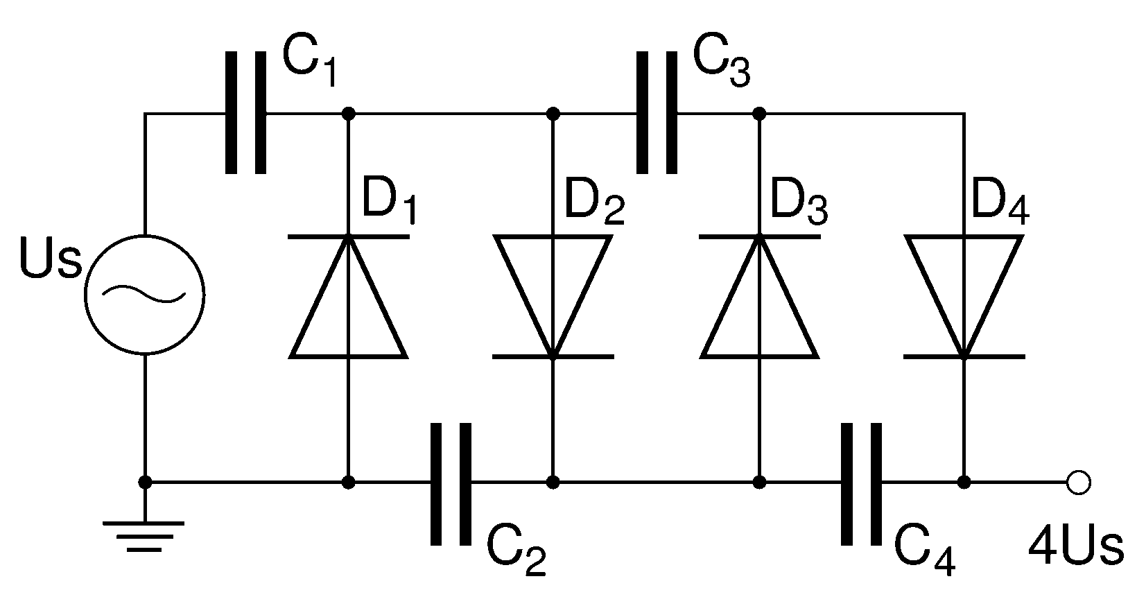
 Villard cascade voltage multiplier.
A voltage multiplier is an electrical circuit that converts AC electrical power from a lower voltage to a higher DC voltage, typically by means of a network of capacitors and diodes.
Voltage multipliers can be used to generate bias voltages ranging from a few volts for electronic appliances, to millions of volts for purposes such as high-energy physics experiments and lightning safety testing.
The most common type of voltage multiplier is the half-wave series multiplier, also called the Villard cascade (but actually invented by Heinrich Greinacher).
Contents
Operation
Assuming that the peak voltage of the AC source is +Us we can describe the (simplified) working of the cascade as follows:
- negative peak (−Us): The C1 capacitor is charged through diode D1 to Us V (potential difference between left and right plate of the capacitor is Us)
- positive peak (+Us): the potential of C1 adds with that of the source, thus charging C2 to 2Us through D2
- negative peak: potential of C1 drops to 0 V thus allowing C3 to be charged through D3 to 2Us.
- positive peak: potential of C1 rises to 2Us (analogously to step 2), also charging C4 to 2Us. The output voltage (the sum of voltages under C2 and C4) raises till 4Us.
In reality more cycles are required for C4 to reach the full voltage. Each additional stage of two diodes and two capacitors increases the output voltage by twice the peak AC supply voltage.
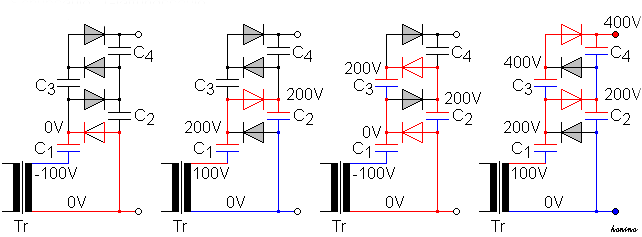
Breakdown voltage
While the multiplier can be used to produce thousands of volts of output, the individual components do not need to be rated to withstand the entire voltage range. Each component only needs to be concerned with the relative voltage differences directly across its own terminals and of the components immediately adjacent to it.
Typically a voltage multiplier will be physically arranged like a ladder, so that the progressively increasing voltage potential is not given the opportunity to arc across to the much lower potential sections of the circuit.
Note that some safety margin is needed across the relative range of voltage differences in the multiplier, so that the ladder can survive the shorted failure of at least one diode or capacitor component. Otherwise a single-point shorting failure could successively over-voltage and destroy each next component in the multiplier, potentially destroying the entire multiplier chain.
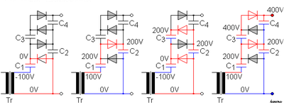
Other circuit topologies
 Two cascades driven by a single center-tapped transformer. This configuration provides full-wave rectification leading to less ripple.
- Stacking
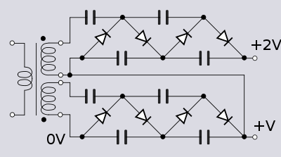 A second cascade stacked onto the first one driven by a high voltage isolated second secondary winding. The second winding is connected with 180° phase shift to get full wave rectification. The two windings need to be insulated against the large voltage between them.
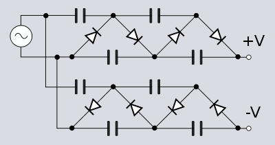 A single secondary winding of a transformer driving two cascades of opposite polarities at the same time. Stacking the two cascades provides an output of twice the voltage but with better ripple and capacitor charging characteristics than would be achieved with a single long cascade of the same voltage.
An even number of diode-capacitor cells is used in any column so that the cascade ends on a smoothing cell. If it were odd and ended on a clamping cell the ripple voltage would be very large. Larger capacitors in the connecting column also reduce ripple but at the expense of charging time and increased diode current.
Dickson charge pump
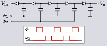 Standard Dickson charge pump. 4-stage (x5 multiplier)
The Dickson charge pump, or Dickson multiplier, is a modification of the Greinacher/Cockcroft-Walton multiplier. Unlike that circuit, however, the Dickson multiplier takes a DC supply as its input so is a form of DC-to-DC converter. Also unlike Greinacher/Cockcroft-Walton which is used on high-voltage applications, the Dickson multiplier is intended for low-voltage purposes. In addition to the DC input, the circuit requires a feed of two clock pulse trains with an amplitude swinging between the DC supply rails. These two pulse trains are opposite phases to each other and non-overlapping so that the switching behaviour is break-before-make.[1]
To describe the ideal operation of the circuit, number the diodes D1, D2 etc. from left to right and the capacitors C1, C2 etc. When the clock
 is low, D1 will charge C1 to Vin. When goes high the top plate of C1 is pushed up to 2Vin. D1 is then turned off and D2 turned on and C2 begins to charge to 2Vin. On the next clock cycle again goes low and now
  goes high pushing the top plate of C2 to 3Vin. D2 switches off and D3 switches on, charging C3 to 3Vin and so on with charge passing up the chain, hence the name charge pump. The final diode-capacitor cell in the cascade is connected to ground rather than a clock phase and hence is not a multiplier; it is a peak detector which merely provides smoothing.[2]
There are a number of factors which reduce the output from the ideal case of nVin. One of these is the threshold voltage, VT of the switching device, that is, the voltage required to turn it on. The output will be reduced by at least nVT due to the volt drops across the switches. Schottky diodes are commonly used in Dickson multipliers for their low forward voltage drop, amongst other reasons. Another difficulty is that there are parasitic capacitances to ground at each node. These parasitic capacitances act as voltage dividers with the circuit's storage capacitors reducing the output voltage still further.[3] Up to a point, a higher clock frequency is beneficial: the ripple is reduced and the high frequency makes the remaining ripple easier to filter. Also the size of capacitors needed is reduced since less charge needs to be stored per cycle. However, losses through stray capacitance increase with increasing clock frequency and a practical limit is around a few hundred kilohertz.[4]
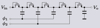 Dickson charge pump using diode-wired MOSFETs. 4-stage (x5 multiplier)
Dickson multipliers are frequently found in integrated circuits (ICs) where they are used to increase a low-voltage battery supply to the voltage needed by the IC. It is advantageous to the IC designer and manufacturer to be able to use the same technology and the same basic device throughout the IC. For this reason, in the popular CMOS technology ICs the transistor which forms the basic building block of circuits is the MOSFET. Consequently, the diodes in the Dickson multiplier are often replaced with MOSFETs wired to behave as diodes.[5]
 Dickson charge pump with linear MOSFET in parallel with diode-wired MOSFET. 4-stage (x5 multiplier)
The diode-wired MOSFET version of the Dickson multiplier does not work very well at very low voltages because of the large drain-source volt drops of the MOSFETs. Frequently, a more complex circuit is used to overcome this problem. One solution is to connect in parallel with the switching MOSFET another MOSFET biased into its linear region. This second MOSFET has a lower drain-source voltage than the switching MOSFET would have on its own (because the switching MOSFET is driven hard on) and consequently the output voltage is increased. The gate of the linear biased MOSFET is connected to the output of the next stage so that it is turned off while the next stage is charging from the previous stage's capacitor. That is, the linear-biased transistor is turned off at the same time as the switching transistor.[6]
An ideal 4-stage Dickson multiplier (x5 multiplier) with an input of 1.5 V would have an output of 7.5 V. However, a diode-wired MOSFET 4-stage multiplier might only have an output of 2 V. Adding parallel MOSFETs in the linear region improves this to around 4 V. More complex circuits still can achieve an output much closer to the ideal case.[7]
Many other variations and improvements to the basic Dickson circuit exist. Some attempt to reduce the switching threshold voltage such as the Mandal-Sarpeshkar multiplier[8] or the Wu multiplier.[9] Other circuits cancel out the threshold voltage: the Umeda multiplier does it with an externally provided voltage[10] and the Nakamoto multiplier with internally generated voltage.[11] The Bergeret multiplier concentrates on maximising power efficiency.[12]
Dickson charge pump modified for RF
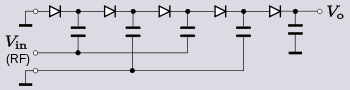 Modified Dickson charge pump. 2-stage (x3 multiplier)
In CMOS integrated circuits clock signals are readily available, or else easily generated. This is not always the case in RF integrated circuits, but often a source of RF power will be available. The standard Dickson multiplier circuit can be modified to meet this requirement by simply grounding the normal input and one of the clock inputs. RF power is injected into the other clock input, which then becomes the circuit input. The RF signal is effectively the clock as well as the source of power. However, since the clock is injected only into every other node the circuit only achieves a stage of multiplication for every second diode-capacitor cell. The other diode-capacitor cells are merely acting as peak detectors and smoothing the ripple without increasing the multiplication.[13]
Cross-coupled switched capacitor
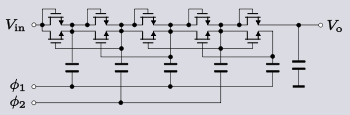
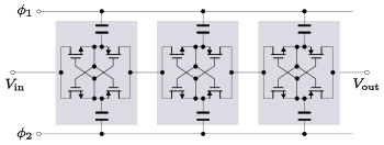 Cascade of cross-coupled MOSFET voltage doublers. 3-stage (x4 multiplier)
A voltage multiplier may be formed of a cascade of voltage doublers of the cross-coupled switched capacitor type. This type of circuit is typically used instead of a Dickson multiplier when the source voltage is 1.2 V or less. Dickson multipliers have increasingly poor power conversion efficiency as the input voltage drops because the voltage drop across the diode-wired transistors becomes much more significant compared to the output voltage. Since the transistors in the cross-coupled circuit are not diode-wired the volt-drop problem is not so serious.[14]
The circuit works by alternately switching the output of each stage between a voltage doubler driven by
and one driven by . This behaviour leads to another advantage over the Dickson multiplier; reduced ripple voltage at double the frequency. The increase in ripple frequency is advantageous because it is easier to remove by filtering. Each stage (in an ideal circuit) raises the output voltage by the peak clock voltage. Assuming that this is the same level as the DC input voltage then an n stage multiplier will (ideally) output nVin. The chief cause of losses in the cross-coupled circuit is parasitic capacitance rather than switching threshold voltage. This causes losses because some of the energy has to go into charging up the stray capacitances on each cycle.[15]Applications
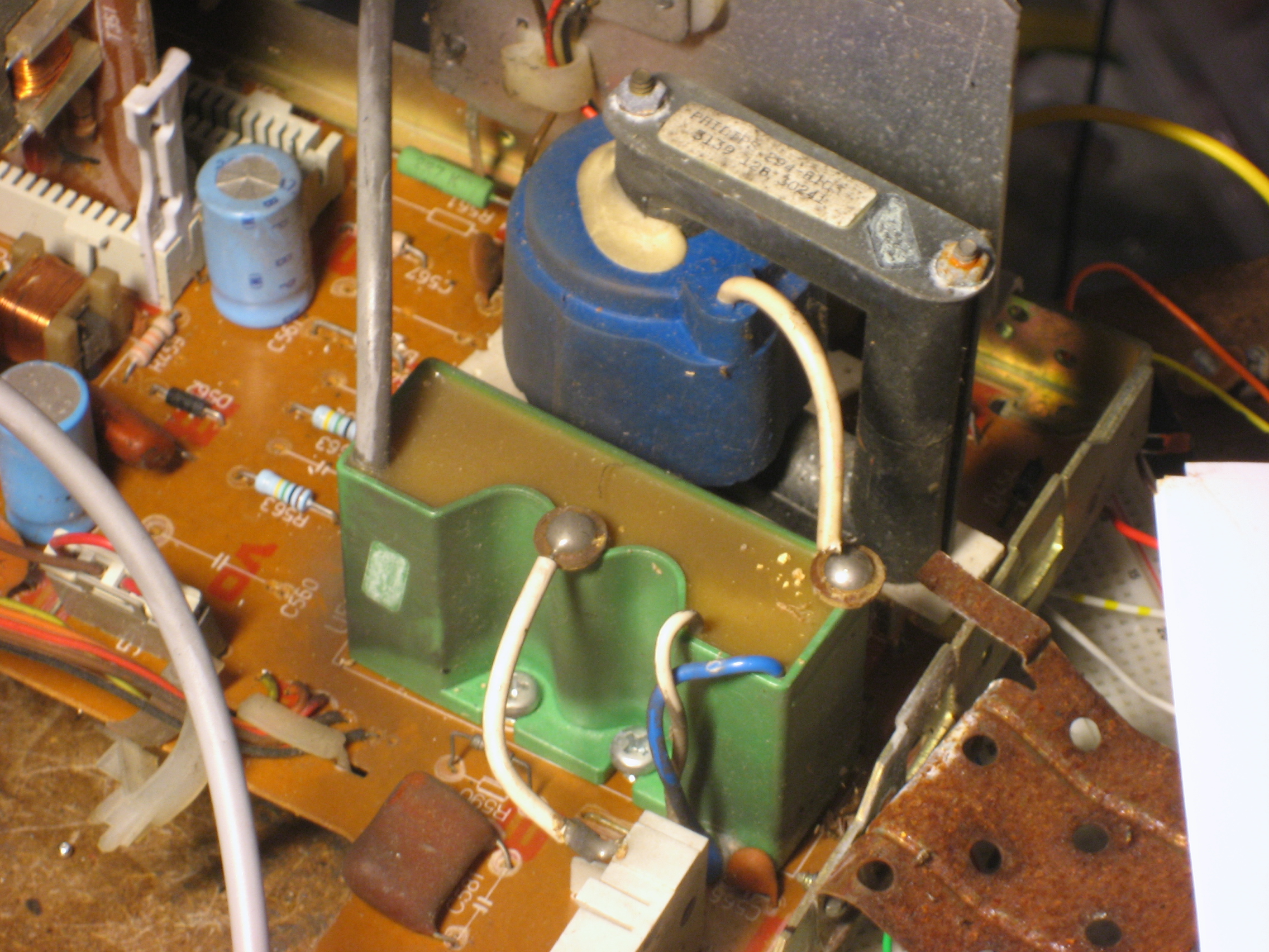
 TV cascade (green) and flyback transformer (blue).
The high-voltage supplies for cathode ray tubes often use voltage multipliers with the final-stage smoothing capacitor formed by the interior and exterior aquadag coatings on the CRT itself.
A common type of voltage multiplier used in high-energy physics is the Cockcroft–Walton generator (which was designed by John Douglas Cockcroft and Ernest Thomas Sinton Walton for a particle accelerator, for use in research that won them the Nobel Prize in Physics in 1951).
See also
- Marx generator (a device that uses spark gaps instead of diodes as the switching elements and can deliver higher peak currents than diodes can)
- Rectifier
- Voltage doubler
- Voltage tripler
Notes
- ^ Liu, p.226
Yuan, p.14 - ^ Liu, p.226-227
- ^ Yuan, pp.13-14
Liu, pp.227-228 - ^ Peluso et al. p.35
Zumbahlen, p.741 - ^ Liu, pp.226-228
Yuan, p.14 - ^ Liu, pp.228-230
Yuan, pp.14-16 - ^ Yuan, pp.14-16
- ^ Yuan, pp.17-18
- ^ Liu, pp.230-232
- ^ Yuan, pp.18-20
- ^ Yuan, pp.19-20
- ^ Yuan, pp.20-21
- ^ Liu, pp.228-230
Yuan, pp.14-15 - ^ Campardo et al., pp.377-379
Liu, pp.232-235
Lin, p.81 - ^ Campardo et al., p.379
Liu, p.234
Bibliography
- Campardo, Giovanni; Micheloni, Rino; Novosel, David VLSI-design of Non-volatile Memories, Springer, 2005 ISBN 354020198X.
- Lin, Yu-Shiang Low Power Circuits for Miniature Sensor Systems, Publisher ProQuest, 2008 ISBN 0549986723.
- Liu, Mingliang Demystifying Switched Capacitor Circuits, Newnes, 2006 ISBN 0750679077.
- Peluso, Vincenzo; Steyaert, Michiel; Sansen, Willy M. C. Design of Low-voltage Low-power CMOS Delta-Sigma A/D Converters, Springer, 1999 ISBN 0792384172.
- Yuan, Fei CMOS Circuits for Passive Wireless Microsystems, Springer, 2010 ISBN 1441976795.
- Zumbahlen, Hank Linear Circuit Design Handbook, Newnes, 2008 ISBN 0750687037.
External links
- Basic multiplier circuits
- Cockcroft Walton multipliers
- Schematic of Kadette brand (International Radio Corp.) model 1019. A 1937 radio with a vacuum tube (25Z5) voltage multiplier rectifier.
Categories:- Electrical circuits
- Electrical power conversion


Wikimedia Foundation. 2010.