- Current mirror
-
A current mirror is a circuit designed to copy a current through one active device by controlling the current in another active device of a circuit, keeping the output current constant regardless of loading. The current being 'copied' can be, and sometimes is, a varying signal current. Conceptually, an ideal current mirror is simply an ideal inverting current amplifier that reverses the current direction as well or it is a current-controlled current source (CCCS). The current mirror is used to provide bias currents and active loads to circuits.
Contents
Mirror characteristics
There are three main specifications that characterize a current mirror. The first is the transfer ratio (in the case of a current amplifier) or the output current magnitude (in the case of a constant current source CCS). The second is its AC output resistance, which determines how much the output current varies with the voltage applied to the mirror. The third specification is the minimum voltage drop across the output part of the mirror necessary to make it work properly. This minimum voltage is dictated by the need to keep the output transistor of the mirror in active mode. The range of voltages where the mirror works is called the compliance range and the voltage marking the boundary between good and bad behavior is called the compliance voltage. There are also a number of secondary performance issues with mirrors, for example, temperature stability.
Practical approximations
For small-signal analysis the current mirror can be approximated by its equivalent Norton impedance .
In large-signal hand analysis, a current mirror is usually and simply approximated by an ideal current source. However, an ideal current source is unrealistic in several respects:
- it has infinite AC impedance, while a practical mirror has finite impedance
- it provides the same current regardless of voltage, that is, there are no compliance range requirements
- it has no frequency limitations, while a real mirror has limitations due to the parasitic capacitances of the transistors
- the ideal source has no sensitivity to real-world effects like noise, power-supply voltage variations and component tolerances.
Circuit realizations of current mirrors
Basic idea
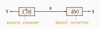

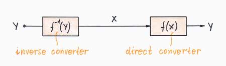
A current mirror consists of two cascaded inverse converters with mirrored transfer characteristic. A bipolar transistor can be used as the simplest current-to-current converter but its transfer ratio would highly depend on temperature variations, β tolerances, etc. To eliminate these undesired disturbances, a current mirror is composed of two cascaded current-to-voltage and voltage-to-current converters placed at the same conditions and having reverse characteristics. They have not to be obligatory linear; the only requirement is their characteristics to be mirrorlike (for example, in the BJT current mirror below, they are logarithmic and exponential). Usually, two identical converters are used but the characteristic of the first one is reversed by applying a negative feedback. Thus a current mirror consists of two cascaded equal converters (the first - reversed and the second - direct).
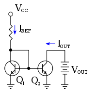 Figure 1: A current mirror implemented with npn bipolar transistors using a resistor to set the reference current IREF; VCC = supply voltage
Basic BJT current mirror
If a voltage is applied to the BJT base-emitter junction as an input quantity and the collector current is taken as an output quantity, the transistor will act as an exponential voltage-to-current converter. By applying a negative feedback (simply joining the base and collector) the transistor can be "reversed" and it will begin acting as the opposite logarithmic current-to-voltage converter; now it will adjust the "output" base-emitter voltage so as to pass the applied "input" collector current.
The simplest bipolar current mirror (shown in Figure 1) implements this idea. It consists of two cascaded transistor stages acting accordingly as a reversed and direct voltage-to-current converters. Transistor Q1 is connected to ground. Its collector-base voltage is zero as shown. Consequently, the voltage drop across Q1 is VBE, that is, this voltage is set by the diode law and Q1 is said to be diode connected. (See also Ebers-Moll model.) It is important to have Q1 in the circuit instead of a simple diode, because Q1 sets VBE for transistor Q2. If Q1 and Q2 are matched, that is, have substantially the same device properties, and if the mirror output voltage is chosen so the collector-base voltage of Q2 is also zero, then the VBE-value set by Q1 results in an emitter current in the matched Q2 that is the same as the emitter current in Q1. Because Q1 and Q2 are matched, their β0-values also agree, making the mirror output current the same as the collector current of Q1. The current delivered by the mirror for arbitrary collector-base reverse bias VCB of the output transistor is given by (see bipolar transistor):
-
 ,
,
where IS = reverse saturation current or scale current, VT = thermal voltage and VA = Early voltage. This current is related to the reference current IREF when the output transistor VCB = 0 V by:
as found using Kirchhoff's current law at the collector node of Q1:
-
- IREF = IC + IB1 + IB2.
The reference current supplies the collector current to Q1 and the base currents to both transistors — when both transistors have zero base-collector bias, the two base currents are equal, IB1=IB2=IB.
Parameter β0 is the transistor β-value for VCB = 0 V.
Output resistance
If VCB is greater than zero in output transistor Q2, the collector current in Q2 will be somewhat larger than for Q1 due to the Early effect. In other words, the mirror has a finite output (or Norton) resistance given by the rO of the output transistor, namely (see Early effect):
-
 ,
,
where VA = Early voltage and VCB = collector-to-base bias.
Compliance voltage
To keep the output transistor active, VCB ≥ 0 V. That means the lowest output voltage that results in correct mirror behavior, the compliance voltage, is VOUT = VCV = VBE under bias conditions with the output transistor at the output current level IC and with VCB = 0 V or, inverting the I-V relation above:
where VT = thermal voltage and IS = reverse saturation current or scale current.
Extensions and complications
When Q2 has VCB > 0 V, the transistors no longer are matched. In particular, their β-values differ due to the Early effect, with
where VA is the Early voltage and β0 = transistor β for VCB = 0 V. Besides the difference due to the Early effect, the transistor β-values will differ because the β0-values depend on current, and the two transistors now carry different currents (see Gummel-Poon model).
Further, Q2 may get substantially hotter than Q1 due to the associated higher power dissipation. To maintain matching, the temperature of the transistors must be nearly the same. In integrated circuits and transistor arrays where both transistors are on the same die, this is easy to achieve. But if the two transistors are widely separated, the precision of the current mirror is compromised.
Additional matched transistors can be connected to the same base and will supply the same collector current. In other words, the right half of the circuit can be duplicated several times with various resistor values replacing R2 on each. Note, however, that each additional right-half transistor "steals" a bit of collector current from Q1 due to the non-zero base currents of the right-half transistors. This will result in a small reduction in the programmed current.
An example of a mirror with emitter degeneration to increase mirror resistance is found in two-port networks.
For the simple mirror shown in the diagram, typical values of β will yield a current match of 1% or better.
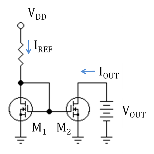
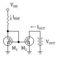 Figure 2: An n-channel MOSFET current mirror with a resistor to set the reference current IREF; VDD is the supply voltage
Basic MOSFET current mirror
The basic current mirror can also be implemented using MOSFET transistors, as shown in Figure 2. Transistor M1 is operating in the saturation or active mode, and so is M2. In this setup, the output current IOUT is directly related to IREF, as discussed next.
The drain current of a MOSFET ID is a function of both the gate-source voltage and the drain-to-gate voltage of the MOSFET given by ID = f (VGS, VDG), a relationship derived from the functionality of the MOSFET device. In the case of transistor M1 of the mirror, ID = IREF. Reference current IREF is a known current, and can be provided by a resistor as shown, or by a "threshold-referenced" or "self-biased" current source to ensure that it is constant, independent of voltage supply variations.[1]
Using VDG=0 for transistor M1, the drain current in M1 is ID = f (VGS,VDG=0), so we find: f (VGS, 0) = IREF, implicitly determining the value of VGS. Thus IREF sets the value of VGS. The circuit in the diagram forces the same VGS to apply to transistor M2. If M2 is also biased with zero VDG and provided transistors M1 and M2 have good matching of their properties, such as channel length, width, threshold voltage etc., the relationship IOUT = f (VGS,VDG=0 ) applies, thus setting IOUT = IREF; that is, the output current is the same as the reference current when VDG=0 for the output transistor, and both transistors are matched.
The drain-to-source voltage can be expressed as VDS=VDG +VGS. With this substitution, the Shichman-Hodges model provides an approximate form for function f (VGS,VDG):[2]
where, Kp is a technology related constant associated with the transistor, W/L is the width to length ratio of the transistor, VGS is the gate-source voltage, Vth is the threshold voltage, λ is the channel length modulation constant, and VDS is the drain source voltage.
Output resistance
Because of channel-length modulation, the mirror has a finite output (or Norton) resistance given by the ro of the output transistor, namely (see channel length modulation):
-
 ,
,
where λ = channel-length modulation parameter and VDS = drain-to-source bias.
Compliance voltage
To keep the output transistor resistance high, VDG ≥ 0 V.[nb 1] (see Baker).[3] That means the lowest output voltage that results in correct mirror behavior, the compliance voltage, is VOUT = VCV = VGS for the output transistor at the output current level with VDG = 0 V, or using the inverse of the f-function, f −1:
-
 .
.
For Shichman-Hodges model, f -1 is approximately a square-root function.
Extensions and reservations
A useful feature of this mirror is the linear dependence of f upon device width W, a proportionality approximately satisfied even for models more accurate than the Shichman-Hodges model. Thus, by adjusting the ratio of widths of the two transistors, multiples of the reference current can be generated.
It must be recognized that the Shichman-Hodges model[4] is accurate only for rather dated technology, although it often is used simply for convenience even today. Any quantitative design based upon new technology uses computer models for the devices that account for the changed current-voltage characteristics. Among the differences that must be accounted for in an accurate design is the failure of the square law in Vgs for voltage dependence and the very poor modeling of Vds drain voltage dependence provided by λVds. Another failure of the equations that proves very significant is the inaccurate dependence upon the channel length L. A significant source of L-dependence stems from λ, as noted by Gray and Meyer, who also note that λ usually must be taken from experimental data.[5]
Feedback assisted current mirror
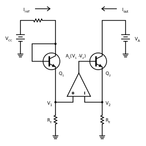 Figure 3: Gain-boosted current mirror with op amp feedback to increase output resistance
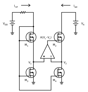 Figure 4: MOSFET version of wide-swing current mirror; M1 and M2 are in active mode, while M3 and M4 are in Ohmic mode and act like resistors
Figure 3 shows a mirror using negative feedback to increase output resistance. Because of the op amp, these circuits are sometimes called gain-boosted current mirrors. Because they have relatively low compliance voltages, they also are called wide-swing current mirrors. A variety of circuits based upon this idea are in use,[6][7][8] particularly for MOSFET mirrors because MOSFETs have rather low intrinsic output resistance values. A MOSFET version of Figure 3 is shown in Figure 4 where MOSFETs M3 and M4 operate in Ohmic mode to play the same role as emitter resistors RE in Figure 3, and MOSFETs M1 and M2 operate in active mode in the same roles as mirror transistors Q1 and Q2 in Figure 3. An explanation follows of how the circuit in Figure 3 works.
The operational amplifier is fed the difference in voltages V1 - V2 at the top of the two emitter-leg resistors of value RE. This difference is amplified by the op amp and fed to the base of output transistor Q2. If the collector base reverse bias on Q2 is increased by increasing the applied voltage VA, the current in Q2 increases, increasing V2 and decreasing the difference V1 - V2 entering the op amp. Consequently, the base voltage of Q2 is decreased, and VBE of Q2 decreases, counteracting the increase in output current.
If the op amp gain Av is large, only a very small difference V1 - V2 is sufficient to generate the needed base voltage VB for Q2, namely
Consequently, the currents in the two leg resistors are held nearly the same, and the output current of the mirror is very nearly the same as the collector current IC1 in Q1, which in turn is set by the reference current as
where β1 for transistor Q1 and β2 for Q2 differ due to the Early effect if the reverse bias across the collector-base of Q2 is non-zero.
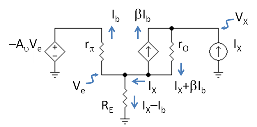
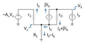 Figure 5: Small-signal circuit to determine output resistance of mirror; transistor Q2 is replaced with its hybrid-pi model; a test current IX at the output generates a voltage VX, and the output resistance is Rout = VX / IX.
Output resistance
An idealized treatment of output resistance is given in the footnote.[nb 2] A small-signal analysis for an op amp with finite gain Av but otherwise ideal is based upon Figure 5 (β, rO and rπ refer to Q2). To arrive at Figure 5, notice that the positive input of the op amp in Figure 3 is at AC ground, so the voltage input to the op amp is simply the AC emitter voltage Ve applied to its negative input, resulting in a voltage output of −Av Ve. Using Ohm's law across the input resistance rπ determines the small-signal base current Ib as:
Combining this result with Ohm's law for RE, Ve can be eliminated, to find:[nb 3]
Kirchhoff's voltage law from the test source IX to the ground of RE provides:
Substituting for Ib and collecting terms the output resistance Rout is found to be:
For a large gain Av >> rπ / RE the maximum output resistance obtained with this circuit is
a substantial improvement over the basic mirror where Rout = rO.
The small-signal analysis of the MOSFET circuit of Figure 4 is obtained from the bipolar analysis by setting β = gm rπ in the formula for Rout and then letting rπ → ∞. The result is
This time, RE is the resistance of the source-leg MOSFETs M3, M4. Unlike Figure 3, however, as Av is increased (holding RE fixed in value), Rout continues to increase, and does not approach a limiting value at large Av.
Compliance voltage
For Figure 3, a large op amp gain achieves the maximum Rout with only a small RE. A low value for RE means V2 also is small, allowing a low compliance voltage for this mirror, only a voltage V2 larger than the compliance voltage of the simple bipolar mirror. For this reason this type of mirror also is called a wide-swing current mirror, because it allows the output voltage to swing low compared to other types of mirror that achieve a large Rout only at the expense of large compliance voltages.
With the MOSFET circuit of Figure 4, like the circuit in Figure 3, the larger the op amp gain Av, the smaller RE can be made at a given Rout, and the lower the compliance voltage of the mirror.
Other current mirrors
There are many sophisticated current mirrors that have higher output resistances than the basic mirror (more closely approach an ideal mirror with current output independent of output voltage) and produce currents less sensitive to temperature and device parameter variations and to circuit voltage fluctuations. These multi-transistor mirror circuits are used both with bipolar and MOS transistors. These circuits include:
- the Widlar current source
- the Wilson current source
- the Cascoded current sources
Notes
- ^ Keeping the output resistance high means more than keeping the MOSFET in active mode, because the output resistance of real MOSFETs only begins to increase on entry into the active region, then rising to become close to maximum value only when VDG ≥ 0 V.
- ^ An idealized version of the argument in the text, valid for infinite op amp gain, is as follows. If the op amp is replaced by a nullor, voltage V2 = V1, so the currents in the leg resistors are held at the same value. That means the emitter currents of the transistors are the same. If the VCB of Q2 increases, so does the output transistor β because of the Early effect: β = β0 ( 1 + VCB / VA ). Consequently the base current to Q2 given by IB = IE / (β + 1) decreases and the output current Iout = IE / (1 + 1 / β) increases slightly because β increases slightly. Doing the math,
-
- ^ Notice that as Av → ∞, Ve → 0 and Ib → IX.
See also
- Current source
- Widlar current source
- Wilson current source
- Bipolar junction transistor
- MOSFET
- Channel length modulation
- Early effect
- {{nmos current mirror{}
References
- ^ Paul R. Gray, Paul J. Hurst, Stephen H. Lewis, Robert G. Meyer (2001). Analysis and Design of Analog Integrated Circuits (Fourth Edition ed.). New York: Wiley. p. 308–309. ISBN 0471321680.
- ^ Gray et al.. Eq. 1.165, p. 44. ISBN 0471321680.
- ^ R. Jacob Baker (2010). CMOS Circuit Design, Layout and Simulation (Third ed.). New York: Wiley-IEEE. pp. 297, §9.2.1 and Figure 20.28, p. 636. ISBN 978-0-470-88132-3.
- ^ NanoDotTek Report NDT14-08-2007, 12 August 2007
- ^ Gray et al.. p. 44. ISBN 0471321680.
- ^ R. Jacob Baker. § 20.2.4 pp. 645–646. ISBN 978-0-470-88132-3.
- ^ Ivanov VI and Filanovksy IM (2004). Operational amplifier speed and accuracy improvement: analog circuit design with structural methodology (The Kluwer international series in engineering and computer science, v. 763 ed.). Boston, Mass.: Kluwer Academic. p. §6.1, p. 105–108. ISBN 1-4020-7772-6. http://books.google.com/books?id=IuLsny9wKIIC&pg=PA110&dq=gain+boost+wide++%22current+mirror%22#PPA107,M1.
- ^ W. M. C. Sansen (2006). Analog design essentials. New York ; Berlin: Springer. p. §0310, p. 93. ISBN 0-387-25746-2.
External links
- Patent (1968) by RJ Widlar: Biasing scheme especially suited for integrated circuits
- Current mirrors
- 4QD tec - Current sources and mirrors Compendium of circuits and descriptions
Categories:- Analog circuits
- Electronic design


Wikimedia Foundation. 2010.