- Photonic crystal
-
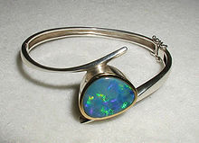 The opal in this bracelet contains a natural periodic microstructure responsible for its iridescent color. It is essentially a natural photonic crystal, although it does not have a complete photonic band gap.
Photonic crystals are periodic optical nanostructures that are designed to affect the motion of photons in a similar way that periodicity of a semiconductor crystal affects the motion of electrons. Photonic crystals occur in nature and in various forms have been studied scientifically for the last 100 years.
Contents
Introduction
Photonic crystals are composed of periodic dielectric or metallo-dielectric nanostructures that affect the propagation of electromagnetic waves (EM) in the same way as the periodic potential in a semiconductor crystal affects the electron motion by defining allowed and forbidden electronic energy bands. Essentially, photonic crystals contain regularly repeating internal regions of high and low dielectric constant. Photons (behaving as waves) propagate through this structure - or not - depending on their wavelength. Wavelengths of light that are allowed to travel are known as modes, and groups of allowed modes form bands. Disallowed bands of wavelengths are called photonic band gaps. This gives rise to distinct optical phenomena such as inhibition of spontaneous emission, high-reflecting omni-directional mirrors and low-loss-waveguiding, amongst others.
Since the basic physical phenomenon is based on diffraction, the periodicity of the photonic crystal structure has to be of the same length-scale as half the wavelength of the EM waves i.e. ~350 nm (blue) to 700 nm (red) for photonic crystals operating in the visible part of the spectrum - the repeating regions of high and low dielectric constants have to be of this dimension. This makes the fabrication of optical photonic crystals cumbersome and complex.
History of photonic crystals
Although photonic crystals have been studied in one form or another since 1887, the term "photonic crystal" was first used over 100 years later, after Eli Yablonovitch and Sajeev John published two milestone papers on photonic crystals in 1987.[1][2]
Before 1987, one-dimensional photonic crystals in the form of periodic multi-layers dielectric stacks (such as the Bragg mirror) were studied extensively. Lord Rayleigh started their study in 1887,[3] by showing that such systems have a one-dimensional photonic band-gap, a spectral range of large reflectivity, known as a stop-band. Today, such structures are used in a diverse range of applications; from reflective coatings to enhancing the efficiency of LEDs to highly reflective mirrors in certain laser cavities (see, for example, VCSEL). A detailed theoretical study of one-dimensional optical structures was performed by Vladimir P. Bykov,[4] who was the first to investigate the effect of a photonic band-gap on the spontaneous emission from atoms and molecules embedded within the photonic structure. Bykov also speculated as to what could happen if two- or three-dimensional periodic optical structures were used.[5] The concept of three-dimensional photonic crystals was then discussed by Ohtaka in 1979,[6] who also developed a formalism for the calculation of the photonic band structure. However, these ideas did not take off until after the publication of two milestone papers in 1987 by Yablonovitch and John. Both these papers concerned high dimensional periodic optical structures – photonic crystals. Yablonovitch's main motivation was to engineer the photonic density of states, to control the spontaneous emission of materials embedded within the photonic crystal; John's idea was to use photonic crystals to affect the localisation and control of light.
After 1987, the number of research papers concerning photonic crystals began to grow exponentially. However, due to the difficulty of actually fabricating these structures at optical scales (see Fabrication Challenges), early studies were either theoretical or in the microwave regime, where photonic crystals can be built on the far more readily accessible centimetre scale. (This fact is due to a property of the electromagnetic fields known as scale invariance – in essence, the electromagnetic fields, as the solutions to Maxwell's equations, has no natural length scale, and so solutions for centimetre scale structure at microwave frequencies are the same as for nanometre scale structures at optical frequencies.) By 1991, Yablonovitch had demonstrated the first three-dimensional photonic band-gap in the microwave regime.[7] The structure that Yablonvitch was able to produce involved drilling an array of holes in a transparent material, where the holes of each layer form an inverse diamond structure - today it is known as Yablonovite.
In 1996, Thomas Krauss made the first demonstration of a two-dimensional photonic crystal at optical wavelengths.[8] This opened up the way for photonic crystals to be fabricated in semiconductor materials by borrowing the methods used in the semiconductor industry. Today, such techniques use photonic crystal slabs, which are two dimensional photonic crystals "etched" into slabs of semiconductor; total internal reflection confines light to the slab, and allows photonic crystal effects, such as engineering the photonic dispersion to be used in the slab. Research is underway around the world to use photonic crystal slabs in integrated computer chips, to improve the optical processing of communications both on-chip and between chips.
Although such techniques have yet to mature into commercial applications, two-dimensional photonic crystals have found commercial use in the form of photonic crystal fibres (otherwise known as holey fibres, because of the air holes that run through them). Photonic crystal fibres were first developed by Philip Russell in 1998, and can be designed to possess enhanced properties over (normal) optical fibres.
The study of three-dimensional photonic crystals has proceeded more slowly than their two-dimensional counterparts. This is because of the increased difficulty in fabrication; there was no inheritance of readily applicable techniques from the semiconductor industry for fabricators of three-dimensional photonic crystals to draw on. Attempts have been made, however, to adapt some of the same techniques, and quite advanced examples have been demonstrated,[9] for example in the construction of "woodpile" structures constructed on a planar layer-by-layer basis. Another strand of research has been to try and construct three-dimensional photonic structures from self-assembly – essentially allowing a mixture of dielectric nano-spheres to settle from solution into three-dimensionally periodic structures possessing photonic band-gaps. The first demonstration of such "inverse opal" structures came in 2000 by researchers at the University of Toronto, Canada.[10] The ever expanding field of biomimetics - the study of structures from nature in order to better understand and use them in design - is also helping researchers in photonic crystals.[11] For example, in 2006 a naturally-occurring photonic crystal was discovered in scales of a Brazilian beetle.[12]
Construction strategies
The fabrication method depends on the number of dimensions that the photonic bandgap must exist in.
One-dimensional photonic crystals
In a one-dimensional photonic crystal, layers of different dielectric constant may be deposited or adhered together to form a band gap in a single direction. A Bragg grating is an example of this type of photonic crystal. One-dimensional photonic crystals can be either isotropic or anisotropic, with the latter having potential use as an optical switch.[13]
Two-dimensional photonic crystals
In two dimensions, holes may be drilled in a substrate that is transparent to the wavelength of radiation that the bandgap is designed to block. Triangular and square latices of holes have been successfully employed.
The Holey fiber or photonic crystal fiber can be made by taking cylindrical rods of glass in hexagonal lattice, and then heating and stretching them, the triangle-like airgaps between the glass rods become the holes that confine the modes.
Three-dimensional photonic crystals
There are several structure types that have been constructed:[14]
- Spheres in a diamond lattice
- Yablonovite
- The Woodpile Structure – "rods" are repeatedly etched using beam lithography, filled in and new material is then deposited thereon, and the process is repeated on the next layer with etched channels that are perpendicular to the layer below, and parallel to and out of phase with the channels two layers below. The process is repeated until the structure is of the desired height. The fill-in material is then dissolved using an agent that can dissolve the fill in material but not the deposition material. It is generally hard to introduce defects into this structure.
- Inverse opals or Inverse Colloidal Crystals-Spheres (such as polystyrene) can be allowed to deposit into a cubic close packed lattice suspended in a solvent. Then a hardener is introduced which makes a transparent solid out of the volume occupied by the solvent. The spheres are then dissolved using an acid such as Hydrochloric acid.
- A stack of two-dimensional crystals - This is a more general class of photonic crystals than Yablonivite, but the original implementation of Yablonovite was created using this method.
Fabrication challenges
The major challenge for higher dimensional photonic crystals is in fabrication of these structures, with sufficient precision to prevent scattering losses blurring the crystal properties and with processes that can be robustly mass produced. One promising method of fabrication for two-dimensionally periodic photonic crystals is a photonic-crystal fiber, such as a "holey fiber". Using fiber draw techniques developed for communications fiber it meets these two requirements, and photonic crystal fibres are commercially available. Another promising method for developing two-dimensional photonic crystals is the so-called photonic crystal slab. These structures consist of a slab of material (such as silicon) which can be patterned using techniques borrowed from the semiconductor industry. Such chips offer the potential to combine photonic processing with electronic processing on a single chip.
For three dimensional photonic crystals various techniques[9] have been used including photolithography and etching techniques similar to those used for integrated circuits. Some of these techniques are already commercially available. To circumvent nanotechnological methods with their complex machinery, alternate approaches have been followed to grow photonic crystals as self-assembled structures from colloidal crystals.
Mass-scale 3D photonic crystal films and fibres can now be produced using a shear-assembly technique which stacks 200-300 nm colloidal polymer spheres into perfect films of fcc lattice. Because the particles have a softer transparent rubber coating the films can be stretched and molded, tuning the photonic bandgaps and producing striking structural color effects.
Computing photonic band structure
The photonic band gap (PBG) is essentially the gap between the air-line and the dielectric-line in the dispersion relation of the PBG system. To design photonic crystal systems, it is essential to engineer the location and size of the bandgap; this is done by computational modeling using any of the following methods.
- Plane wave expansion method
- Finite element method.
- Finite difference time domain method
- Order-n spectral method[15][16]
- KKR method
- Bloch wave – MoM method
Essentially these methods solve for the frequencies (normal models) of the photonic crystal for each value of the propagation direction given by the wave vector, or vice-versa. The various lines in the band structure, correspond to the different cases of n, the band index. For an introduction to photonic band structure, see Joannopoulos.[17]
 Band structure of a 1D Photonic Crystal, DBR air-core calculated using plane wave expansion technique with 101 planewaves, for d/a=0.8, and dielectric contrast of 12.250.
The plane wave expansion method, can be used to calculate the band structure using an eigen formulation of the Maxwell's equations, and thus solving for the eigen frequencies for each of the propagation directions, of the wave vectors. It directly solves for the dispersion diagram. Electric field strength values can also be calculated over the spatial domain of the problem using the eigen vectors of the same problem. For the picture shown to the right, corresponds to the band-structure of a 1D DBR with air-core interleaved with a dielectric material of relative permittivity 12.25, and a lattice period to air-core thickness ratio (d/a) of 0.8, is solved using 101 planewaves over the first irreducible Brillouin zone.
In order to speed up the calculation of the frequency band structure, the Reduced Bloch Mode Expansion (RBME) method can be used.[18] The RBME method applies "on top" of any of the primary expansion methods mentioned above. For large unit cell models, the RBME method can reduce the time for computing the band structure by up to two orders of magnitude.
Applications
Photonic crystals are attractive optical materials for controlling and manipulating the flow of light. One dimensional photonic crystals are already in widespread use in the form of thin-film optics with applications ranging from low and high reflection coatings on lenses and mirrors to colour changing paints and inks. Higher dimensional photonic crystals are of great interest for both fundamental and applied research, and the two dimensional ones are beginning to find commercial applications. The first commercial products involving two-dimensionally periodic photonic crystals are already available in the form of photonic-crystal fibers, which use a microscale structure to confine light with radically different characteristics compared to conventional optical fiber for applications in nonlinear devices and guiding exotic wavelengths. The three-dimensional counterparts are still far from commercialization but offer additional features possibly leading to new device concepts (e.g. optical computers), when some technological aspects such as manufacturability and principal difficulties such as disorder are under control.
See also
- Colloidal crystal
- Left-handed material
- Metamaterial
- Nanotechnology
- Nanomaterials
- Photonic-crystal fiber
- Photonic metamaterials
- Superprism
- Superlens
- Thin-film optics
- Tunable metamaterials
- Optical medium
References
- ^ E. Yablonovitch (1987), "Inhibited Spontaneous Emission in Solid-State Physics and Electronics" (PDF), Physical Review Letters 58 (20): 2059–2062, Bibcode 1987PhRvL..58.2059Y, doi:10.1103/PhysRevLett.58.2059, PMID 10034639, http://www.ee.ucla.edu/faculty/papers/eliy1987PhysRevLett.pdf
- ^ S. John (1987), "Strong localization of photons in certain disordered dielectric superlattices" (PDF), Physical Review Letters 58 (23): 2486–2489, Bibcode 1987PhRvL..58.2486J, doi:10.1103/PhysRevLett.58.2486, PMID 10034761, http://www.physics.utoronto.ca/~john/john/p2486_1.pdf
- ^ J. W. S. Rayleigh (1888), "On the remarkable phenomenon of crystalline reflexion described by Prof. Stokes" (PDF), Phil. Mag 26: 256–265, http://optoelectronics.eecs.berkeley.edu/LordRayleighB.pdf
- ^ V. P. Bykov (1972), "Spontaneous Emission in a Periodic Structure", Soviet Journal of Experimental and Theoretical Physics 35: 269–273, Bibcode 1972JETP...35..269B
- ^ V. P. Bykov (1975), "Spontaneous emission from a medium with a band spectrum", Quantum Electronics 4 (7): 861–871, Bibcode 1975QuEle...4..861B, doi:10.1070/QE1975v004n07ABEH009654, http://www.iop.org/EJ/abstract/0049-1748/4/7/A10
- ^ K. Ohtaka (1979), "Energy band of photons and low-energy photon diffraction", Physical Review B 19 (10): 5057–5067, Bibcode 1979PhRvB..19.5057O, doi:10.1103/PhysRevB.19.5057, http://link.aps.org/doi/10.1103/PhysRevB.19.5057
- ^ E. Yablonovitch, T.J. Gmitter, K.M. Leung, E; Gmitter, TJ; Leung, KM (1991), "Photonic band structure: the face-centered-cubic case employing nonspherical atoms" (PDF), Physical Review Letters 67 (17): 2295–2298, Bibcode 1991PhRvL..67.2295Y, doi:10.1103/PhysRevLett.67.2295, PMID 10044390, http://www.ee.ucla.edu/~photon/pubs/ey1991prl6717.pdf
- ^ T. F. Krauss, R. M. DeLaRue, S. Brand (1996), "Two-dimensional photonic-bandgap structures operating at near-infrared wavelengths", Nature 383 (6602): 699–702, Bibcode 1996Natur.383..699K, doi:10.1038/383699a0
- ^ a b Review: S. Johnson (MIT) Lecture 3: Fabrication technologies for 3d photonic crystals, a survey
- ^ Blanco, Alvaro (2000), "Large-scale synthesis of a silicon photonic crystal with a complete three-dimensional bandgap near 1.5 micrometres", Nature 405 (6785): 437–440, doi:10.1038/35013024, http://www.nature.com/nature/journal/v405/n6785/full/405437a0.html
- ^ Kolle, Mathias (2011), Photonic Structures Inspired by Nature (1st ed.), ISBN 978-3-642-15168-2, http://www.springer.com/physics/condensed+matter+physics/book/978-3-642-15168-2
- ^ Michael H. Bartl et al (2008), "Discovery of a diamond-based photonic crystal structure in beetle scales", Physical Review Letters 77 (5), Bibcode 2008PhRvE..77e0904G, doi:10.1103/PhysRevE.77.050904, http://link.aps.org/doi/10.1103/PhysRevE.77.050904
- ^ Fiddy, Michael A.; Schenk, John O.; Cao, Yang (2008). "Third Order Nonlinear Effect near a Degenerate Band Edge". Optics and Photonics Letters 1 (1): 1–7. doi:10.1142/S1793528808000033.
- ^ http://ab-initio.mit.edu/book/photonic-crystals-book.pdf
- ^ P. Ordejon (1998), "Order-n tight-binding methods for electronic-structure and molecular dynamics", Computational materials science 12 (3): 157–191, doi:10.1016/S0927-0256(98)00027-5, http://cat.inist.fr/?aModele=afficheN&cpsidt=1640567
- ^ Richard M Martin, Linear Scaling 'Order-N' Methods in Electronic Structure Theory
- ^ John D Joannopoulos, Johnson SG, Winn JN & Meade RD (2008), Photonic Crystals: Molding the Flow of Light (2nd ed.), Princeton NJ: Princeton University Press, ISBN 978-0-691-12456-8, http://ab-initio.mit.edu/book/
- ^ M.I. Hussein (2009), "Reduced Bloch mode expansion for periodic media band structure calculations", Proceedings of the Royal Society A 465 (2109): 2825–2848, Bibcode 2009RSPSA.465.2825H, doi:10.1098/rspa.2008.0471, http://rspa.royalsocietypublishing.org/content/465/2109/2825.full
External links
- Business report on Photonic Crystals in Metamaterials - see also Scope and Analyst
- Prof Yablonovitch's Optoelectronics Group at UCLA School of Engineering and Applied Sciences
- Prof John's page at University of Toronto
- Prof Vos's group at University of Twente
- Prof Giessen's group at Universität Stuttgart
- Prof Wegener's group at Universität Karlsruhe (TH)
- Photonic crystals tutorials by Prof S. Johnson at MIT
- Photonic crystals tutorials by Prof Cefe Lopez at ICMM
- Autocloning at Photonic Lattice, Inc
- ePIXnet Nanostructuring Platform for Photonic Integration
- PhOREMOST: Nanophotonics to realise molecular scale technology
- Metamaterials and Photonic Crystals Group at Unidad Asociada ICMM-CSIC/UPV
- Photonic crystals an introduction
- Prof Eich's group at Hamburg University of Technology
- Invisibility cloak created in 3-D; Photonic crystals(BBC)
- Extruded Flexible Polymer Photonics Crystals at Cambridge
Categories:- Condensed matter physics
- Metamaterials
- Photonics
- Optics


Wikimedia Foundation. 2010.