- Scanning tunneling microscope
-
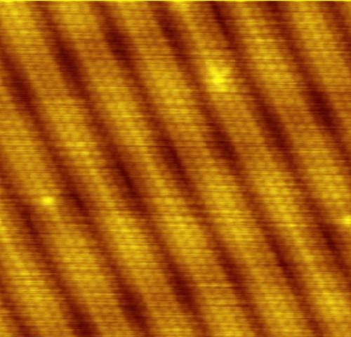
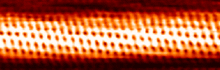 An STM image of a single-walled carbon nanotube
A scanning tunneling microscope (STM) is an instrument for imaging surfaces at the atomic level. Its development in 1981 earned its inventors, Gerd Binnig and Heinrich Rohrer (at IBM Zürich), the Nobel Prize in Physics in 1986.[1][2] For an STM, good resolution is considered to be 0.1 nm lateral resolution and 0.01 nm depth resolution.[3] With this resolution, individual atoms within materials are routinely imaged and manipulated. The STM can be used not only in ultra-high vacuum but also in air, water, and various other liquid or gas ambients, and at temperatures ranging from near zero kelvin to a few hundred degrees Celsius.[4]
The STM is based on the concept of quantum tunneling. When a conducting tip is brought very near to the surface to be examined, a bias (voltage difference) applied between the two can allow electrons to tunnel through the vacuum between them. The resulting tunneling current is a function of tip position, applied voltage, and the local density of states (LDOS) of the sample.[4] Information is acquired by monitoring the current as the tip's position scans across the surface, and is usually displayed in image form. STM can be a challenging technique, as it requires extremely clean and stable surfaces, sharp tips, excellent vibration control, and sophisticated electronics.
Contents
Procedure
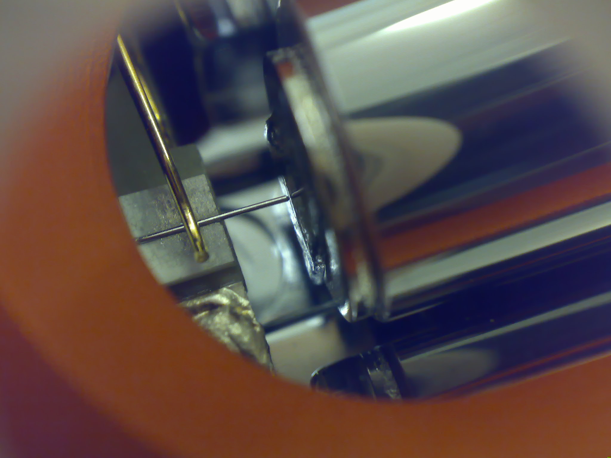
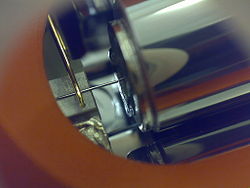 A close-up of a simple scanning tunneling microscope head using a platinum-iridium tip.
First, a voltage bias is applied and the tip is brought close to the sample by some coarse sample-to-tip control, which is turned off when the tip and sample are sufficiently close. At close range, fine control of the tip in all three dimensions when near the sample is typically piezoelectric, maintaining tip-sample separation W typically in the 4-7 Å range, which is the equilibrium position between attractive (3<W<10Å) and repulsive (W<3Å) interactions.[4] In this situation, the voltage bias will cause electrons to tunnel between the tip and sample, creating a current that can be measured. Once tunneling is established, the tip's bias and position with respect to the sample can be varied (with the details of this variation depending on the experiment) and data is obtained from the resulting changes in current.
If the tip is moved across the sample in the x-y plane, the changes in surface height and density of states cause changes in current. These changes are mapped in images. This change in current with respect to position can be measured itself, or the height, z, of the tip corresponding to a constant current can be measured.[4] These two modes are called constant height mode and constant current mode, respectively. In constant current mode, feedback electronics adjust the height by a voltage to the piezoelectric height control mechanism.[5] This leads to a height variation and thus the image comes from the tip topography across the sample and gives a constant charge density surface; this means contrast on the image is due to variations in charge density.[6] In constant height mode, the voltage and height are both held constant while the current changes to keep the voltage from changing; this leads to an image made of current changes over the surface, which can be related to charge density.[6] The benefit to using a constant height mode is that it is faster, as the piezoelectric movements require more time to register the height change in constant current mode, than the voltage change in constant height mode.[6] All images produced by STM are grayscale, with color optionally added in post-processing in order to visually emphasize important features.
In addition to scanning across the sample, information on the electronic structure at a given location in the sample can be obtained by sweeping voltage and measuring current at a specific location.[3] This type of measurement is called scanning tunneling spectroscopy (STS) and typically results in a plot of the local density of states as a function of energy within the sample. The advantage of STM over other measurements of the density of states lies in its ability to make extremely local measurements: for example, the density of states at an impurity site can be compared to the density of states far from impurities.[7]
Framerates of at least 1 Hz enable so called Video-STM (up to 50 Hz is possible).[8][9] This can be used to scan surface diffusion.[10]
Instrumentation
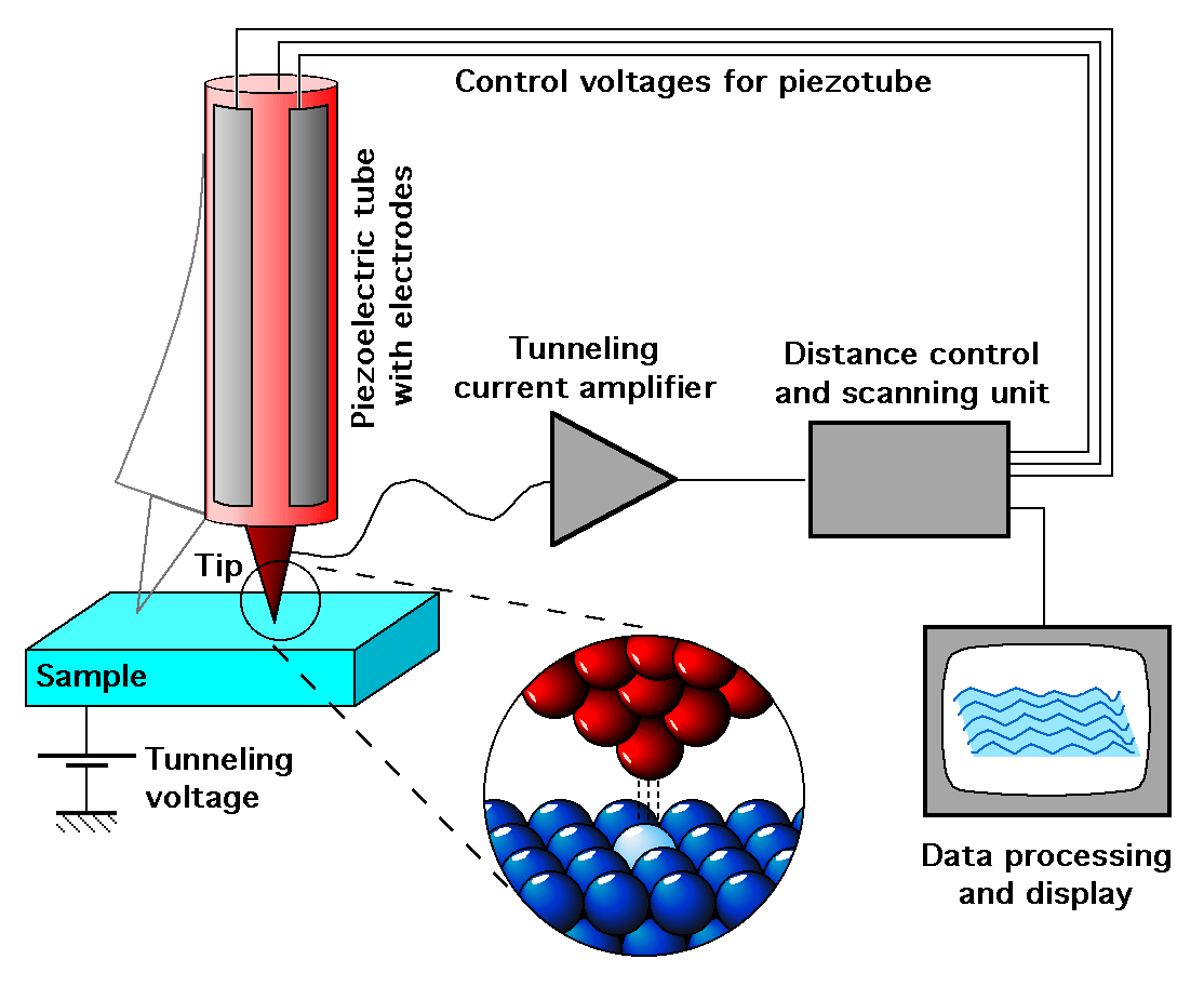
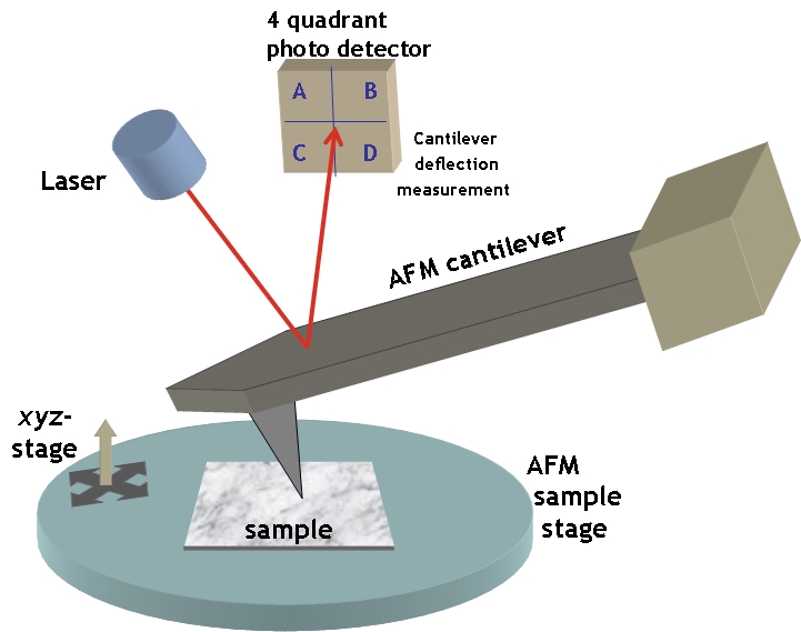
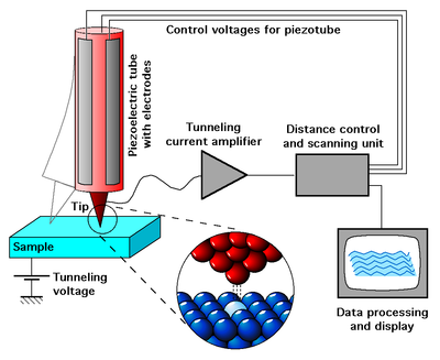 Schematic view of an STM
The components of an STM include scanning tip, piezoelectric controlled height and x,y scanner, coarse sample-to-tip control, vibration isolation system, and computer.[5]
The resolution of an image is limited by the radius of curvature of the scanning tip of the STM.Additionally,image artifacts can occur if the tip has two tips at the end rather than a single atom; this leads to “double-tip imaging,” a situation in which both tips contribute to the tunneling.[3] Therefore it has been essential to develop processes for consistently obtaining sharp, usable tips. Recently, carbon nanotubes have been used in this instance.[11]
The tip is often made of tungsten or platinum-iridium, though gold is also used.[3] Tungsten tips are usually made by electrochemical etching, and platinum-iridium tips by mechanical shearing.[3]
Due to the extreme sensitivity of tunnel current to height, proper vibration isolation or an extremely rigid STM body is imperative for obtaining usable results. In the first STM by Binnig and Rohrer, magnetic levitation was used to keep the STM free from vibrations; now mechanical spring or gas spring systems are often used.[4] Additionally, mechanisms for reducing eddy currents are sometimes implemented.
Maintaining the tip position with respect to the sample, scanning the sample and acquiring the data is computer controlled.[5] The computer may also be used for enhancing the image with the help of image processing[12][13] as well as performing quantitative measurements.[14]
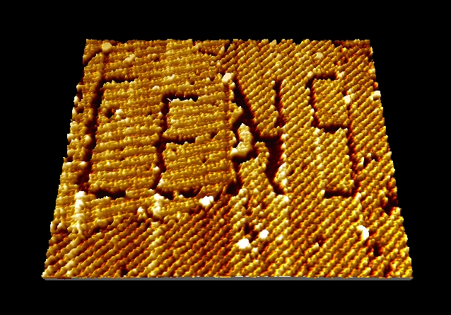
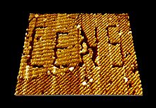 Nanomanipulation via STM of a self-assembled organic semiconductor monolayer (here: PTCDA molecules) on graphite, in which the logo of the Center for NanoScience (CeNS), LMU has been written.
Many other microscopy techniques have been developed based upon STM. These include photon scanning microscopy (PSTM), which uses an optical tip to tunnel photons;[3] scanning tunneling potentiometry (STP), which measures electric potential across a surface;[3] spin polarized scanning tunneling microscopy (SPSTM), which uses a ferromagnetic tip to tunnel spin-polarized electrons into a magnetic sample,[15] and atomic force microscopy (AFM), in which the force caused by interaction between the tip and sample is measured.
Other STM methods involve manipulating the tip in order to change the topography of the sample. This is attractive for several reasons. Firstly the STM has an atomically precise positioning system which allows very accurate atomic scale manipulation. Furthermore, after the surface is modified by the tip, it is a simple matter to then image with the same tip, without changing the instrument. IBM researchers developed a way to manipulate Xenon atoms adsorbed on a nickel surface.[3] This technique has been used to create electron "corrals" with a small number of adsorbed atoms, which allows the STM to be used to observe electron Friedel oscillations on the surface of the material. Aside from modifying the actual sample surface, one can also use the STM to tunnel electrons into a layer of E-Beam photoresist on a sample, in order to do lithography. This has the advantage of offering more control of the exposure than traditional Electron beam lithography. Another practical application of STM is atomic deposition of metals (Au, Ag, W, etc.) with any desired (pre-programmed) pattern, which can be used as contacts to nanodevices or as nanodevices themselves.
Recently groups have found they can use the STM tip to rotate individual bonds within single molecules. The electrical resistance of the molecule depends on the orientation of the bond, so the molecule effectively becomes a molecular switch.
Principle of operation
Tunneling is a functioning concept that arises from quantum mechanics. Classically, an object hitting an impenetrable barrier will not pass through. In contrast, objects with a very small mass, such as the electron, have wavelike characteristics which permit such an event, referred to as tunneling.
Electrons behave as beams of energy, and in the presence of a potential U(z), assuming 1-dimensional case, the energy levels ψn(z) of the electrons are given by solutions to Schrödinger’s equation,
where ħ is the reduced Planck’s constant, z is the position, and m is the mass of an electron.[4] If an electron of energy E is incident upon an energy barrier of height U(z), the electron wave function is a traveling wave solution,
where
if E > U(z), which is true for a wave function inside the tip or inside the sample.[4] Inside a barrier, E < U(z) so the wave functions which satisfy this are decaying waves,
where
quantifies the decay of the wave inside the barrier, with the barrier in the +z direction for − κ.[4]
Knowing the wave function allows one to calculate the probability density for that electron to be found at some location. In the case of tunneling, the tip and sample wave functions overlap such that when under a bias, there is some finite probability to find the electron in the barrier region and even on the other side of the barrier.[4] Let us assume the bias is V and the barrier width is W. This probability, P, that an electron at z=0 (left edge of barrier) can be found at z=W (right edge of barrier) is proportional to the wave function squared,
-
 .[4]
.[4]
If the bias is small, we can let U − E ≈ φM in the expression for κ, where φM, the work function, gives the minimum energy needed to bring an electron from an occupied level, the highest of which is at the Fermi level (for metals at T=0 kelvins), to vacuum level. When a small bias V is applied to the system, only electronic states very near the Fermi level, within eV (a product of electron charge and voltage, not to be confused here with electronvolt unit), are excited.[4] These excited electrons can tunnel across the barrier. In other words, tunneling occurs mainly with electrons of energies near the Fermi level.
However, tunneling does require that there is an empty level of the same energy as the electron for the electron to tunnel into on the other side of the barrier. It is because of this restriction that the tunneling current can be related to the density of available or filled states in the sample. The current due to an applied voltage V (assume tunneling occurs sample to tip) depends on two factors: 1) the number of electrons between Ef and eV in the sample, and 2) the number among them which have corresponding free states to tunnel into on the other side of the barrier at the tip.[4] The higher density of available states the greater the tunneling current. When V is positive, electrons in the tip tunnel into empty states in the sample; for a negative bias, electrons tunnel out of occupied states in the sample into the tip.[4]
Mathematically, this tunneling current is given by
-
 .
.
One can sum the probability over energies between Ef − eV and Ef to get the number of states available in this energy range per unit volume, thereby finding the local density of states (LDOS) near the Fermi level.[4] The LDOS near some energy E in an interval ε is given by
-
 ,
,
and the tunnel current at a small bias V is proportional to the LDOS near the Fermi level, which gives important information about the sample.[4] It is desirable to use LDOS to express the current because this value does not change as the volume changes, while probability density does.[4] Thus the tunneling current is given by
where ρs(0,Ef) is the LDOS near the Fermi level of the sample at the sample surface.[4] This current can also be expressed in terms of the LDOS near the Fermi level of the sample at the tip surface,
The exponential term in the above equations means that small variations in W greatly influence the tunnel current. If the separation is decreased by 1 Ǻ, the current increases by an order of magnitude, and vice versa.[6]
This approach fails to account for the rate at which electrons can pass the barrier. This rate should affect the tunnel current, so it can be treated using the Fermi's golden rule with the appropriate tunneling matrix element. John Bardeen solved this problem in his study of the metal-insulator-metal junction.[16] He found that if he solved Schrödinger’s equation for each side of the junction separately to obtain the wave functions ψ and χ for each electrode, he could obtain the tunnel matrix, M, from the overlap of these two wave functions.[4] This can be applied to STM by making the electrodes the tip and sample, assigning ψ and χ as sample and tip wave functions, respectively, and evaluating M at some surface S between the metal electrodes, where z=0 at the sample surface and z=W at the tip surface.[4]
Now, Fermi’s Golden Rule gives the rate for electron transfer across the barrier, and is written
-
 ,
,
where δ(Eψ–Eχ) restricts tunneling to occur only between electron levels with the same energy.[4] The tunnel matrix element, given by
-
 ,
,
is a description of the lower energy associated with the interaction of wave functions at the overlap, also called the resonance energy.[4]
Summing over all the states gives the tunneling current as
-
![I = \frac{4 \pi e}{\hbar}\int_{-\infty}^{+\infty} [f(E_f -eV + \epsilon) - f(E_f + \epsilon)] \rho_s (E_f - eV + \epsilon) \rho_T (E_f + \epsilon)|M|^2 d \epsilon](d/57d2ee4b5c71bb811c53328157346311.png) ,
,
where f is the Fermi function, ρs and ρT are the density of states in the sample and tip, respectively.[4] The Fermi distribution function describes the filling of electron levels at a given temperature T.
Early invention
An earlier, similar invention, the Topografiner of R. Young, J. Ward, and F. Scire from the NIST,[17] relied on field emission. However, Young is credited by the Nobel Committee as the person who realized that it should be possible to achieve better resolution by using the tunnel effect.[18]
See also
References
- ^ G. Binnig, H. Rohrer (1986). "Scanning tunneling microscopy". IBM Journal of Research and Development 30: 4.
- ^ Press release for the 1986 Nobel Prize in physics
- ^ a b c d e f g h C. Bai (2000). Scanning tunneling microscopy and its applications. New York: Springer Verlag. ISBN 3540657150. http://books.google.com/?id=3Q08jRmmtrkC&pg=PA345.
- ^ a b c d e f g h i j k l m n o p q r s t u v C. Julian Chen (1993). Introduction to Scanning Tunneling Microscopy. Oxford University Press. ISBN 0195071506. http://www.columbia.edu/~jcc2161/documents/STM_2ed.pdf.
- ^ a b c K. Oura, V. G. Lifshits, A. A. Saranin, A. V. Zotov, and M. Katayama (2003). Surface science: an introduction. Berlin: Springer-Verlag. ISBN 3540005455. http://books.google.com/?id=TTPMbOGqF-YC&pg=PP1.
- ^ a b c d D. A. Bonnell and B. D. Huey (2001). "Basic principles of scanning probe microscopy". In D. A. Bonnell. Scanning probe microscopy and spectroscopy: Theory, techniques, and applications (2 ed.). New York: Wiley-VCH. ISBN 047124824X.
- ^ Pan, S. H.; Hudson, EW; Lang, KM; Eisaki, H; Uchida, S; Davis, JC (2000). "Imaging the effects of individual zinc impurity atoms on superconductivity in Bi2Sr2CaCu2O8+delta". Nature 403 (6771): 746–750. arXiv:cond-mat/9909365. Bibcode 2000Natur.403..746P. doi:10.1038/35001534. PMID 10693798.
- ^ G. Schitter, M. J. Rost (2008). "Scanning probe microscopy at video-rate" (PDF). Materials Today (UK: Elsevier) 11 (special issue): 40–48. doi:10.1016/S1369-7021(09)70006-9. ISSN 1369-7021. http://www.materialstoday.com/view/2194/scanning-probe-microscopy-at-videorate/.
- ^ R. V. Lapshin, O. V. Obyedkov (1993). "Fast-acting piezoactuator and digital feedback loop for scanning tunneling microscopes" (PDF). Review of Scientific Instruments 64 (10): 2883–2887. Bibcode 1993RScI...64.2883L. doi:10.1063/1.1144377. http://www.nanoworld.org/homepages/lapshin/publications.htm#fast1993.
- ^ B. S. Swartzentruber (1996). "Direct measurement of surface diffusion using atom-tracking scanning tunneling microscopy". Physical Review Letters 76 (3): 459–462. Bibcode 1996PhRvL..76..459S. doi:10.1103/PhysRevLett.76.459. PMID 10061462.
- ^ "STM carbon nanotube tips fabrication for critical dimension measurements". Sensors and Actuators A 123-124: 655. 2005. doi:10.1016/j.sna.2005.02.036.
- ^ R. V. Lapshin (1995). "Analytical model for the approximation of hysteresis loop and its application to the scanning tunneling microscope" (PDF). Review of Scientific Instruments 66 (9): 4718–4730. Bibcode 1995RScI...66.4718L. doi:10.1063/1.1145314. http://www.nanoworld.org/homepages/lapshin/publications.htm#analytical1995. (Russian translation is available).
- ^ R. V. Lapshin (2007). "Automatic drift elimination in probe microscope images based on techniques of counter-scanning and topography feature recognition" (PDF). Measurement Science and Technology 18 (3): 907–927. Bibcode 2007MeScT..18..907L. doi:10.1088/0957-0233/18/3/046. http://www.nanoworld.org/homepages/lapshin/publications.htm#automatic2007.
- ^ R. V. Lapshin (2004). "Feature-oriented scanning methodology for probe microscopy and nanotechnology" (PDF). Nanotechnology 15 (9): 1135–1151. Bibcode 2004Nanot..15.1135L. doi:10.1088/0957-4484/15/9/006. http://www.nanoworld.org/homepages/lapshin/publications.htm#feature2004.
- ^ R. Wiesendanger, I. V. Shvets, D. Bürgler, G. Tarrach, H.-J. Güntherodt, and J.M.D. Coey (1992). "Recent advances in spin-polarized scanning tunneling microscopy". Ultramicroscopy 42-44: 338. doi:10.1016/0304-3991(92)90289-V.
- ^ J. Bardeen (1961). "Tunneling from a many particle point of view". Phys. Rev. Lett. 6 (2): 57–59. Bibcode 1961PhRvL...6...57B. doi:10.1103/PhysRevLett.6.57.
- ^ R. Young, J. Ward, F. Scire (1972). "The Topografiner: An Instrument for Measuring Surface Microtopography". Rev. Sci. Instrum. 43: 999. doi:10.1063/1.1685846. http://www.nanoworld.org/museum/young2.pdf.
- ^ "The Topografiner: An Instrument for Measuring Surface Microtopography". NIST. http://nvl.nist.gov/pub/nistpubs/sp958-lide/214-218.pdf.
Further reading
- Tersoff, J.: Hamann, D. R.: Theory of the scanning tunneling microscope, Physical Review B 31, 1985, p. 805 - 813.
- Bardeen, J.: Tunnelling from a many-particle point of view, Physical Review Letters 6 (2), 1961, p. 57-59.
- Chen, C. J.: Origin of Atomic Resolution on Metal Surfaces in Scanning Tunneling Microscopy, Physical Review Letters 65 (4), 1990, p. 448-451
- G. Binnig, H. Rohrer, Ch. Gerber, and E. Weibel, Phys. Rev. Lett. 50, 120 - 123 (1983)
- G. Binnig, H. Rohrer, Ch. Gerber, and E. Weibel, Phys. Rev. Lett. 49, 57 - 61 (1982)
- G. Binnig, H. Rohrer, Ch. Gerber, and E. Weibel, Appl. Phys. Lett., Vol. 40, Issue 2, pp. 178-180 (1982)
- R. V. Lapshin, Feature-oriented scanning methodology for probe microscopy and nanotechnology, Nanotechnology, volume 15, issue 9, pages 1135-1151, 2004
- D. Fujita and K. Sagisaka, Topical review: Active nanocharacterization of nanofunctional materials by scanning tunneling microscopy Sci. Technol. Adv. Mater. 9, 013003(9pp) (2008) (free download).
- Roland Wiesendanger (1994). Scanning probe microscopy and spectroscopy: methods and applications. Cambridge University Press. ISBN 0521428475. http://books.google.com/?id=EXae0pjS2vwC&printsec=frontcover.
- Theory of STM and Related Scanning Probe Methods. Springer Series in Surface Sciences, Band 3. Springer, Berlin 1998
External links
- A microscope is filming a microscope (Mpeg, AVI movies)
- Zooming into the NanoWorld (Animation with measured STM images)
- NobelPrize.org website about STM, including an interactive STM simulator.
- SPM - Scanning Probe Microscopy Website
- STM Image Gallery at IBM Almaden Research Center
- STM Gallery at Vienna University of technology
- Build a simple STM with a cost of materials less than $100.00 excluding oscilloscope
- Nanotimes Simulation engine of scanning tunneling microscope
- Structure and Dynamics of Organic Nanostructures discovered by STM
- Metal organic coordination networks of oligopyridines and Cu on graphite investigated by STM
- Surface Alloys discovered by STM
- Animated illustration of tunneling and STM
- 60 second movie clip with an introduction to Scanning Tunneling Microscopy(STM)
Scanning probe microscopy Common Atomic force · Scanning tunneling
Other Electrostatic force · Electrochemical scanning tunneling · Kelvin probe force · Magnetic force · Magnetic resonance force · Near-field scanning optical · Photothermal microspectroscopy · Scanning capacitance · Scanning gate · Scanning Hall probe · Scanning ion-conductance · Spin polarized scanning tunneling · Scanning voltageApplications See also Categories:- Scanning probe microscopy
- Swiss inventions
- Microscopes
-


Wikimedia Foundation. 2010.